Bridging the Frontier Bob Smith, Executive Director
Bob Smith is Executive Director of the ESD Alliance responsible for its management and operations. Previously, Bob was senior vice president of Marketing and Business Development at Uniquify, responsible for brand development, positioning, strategy and business development activities. Bob began his … More » Atomera on Boosting Semiconductor Performance With Quantum-Engineered MaterialsOctober 12th, 2023 by Bob Smith, Executive Director
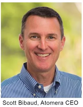
 Atomera, a semiconductor materials and technology licensing company, is the newest member of the ESD Alliance. In welcoming Atomera to our membership, I spoke with Atomera CEO Scott Bibaud to learn more about its atomic-level technology that enhances transistors to improve performance in electronic products. We also discussed quantum-engineered materials and their impact on chip performance, recruiting and industry trends. Atomera, a semiconductor materials and technology licensing company, is the newest member of the ESD Alliance. In welcoming Atomera to our membership, I spoke with Atomera CEO Scott Bibaud to learn more about its atomic-level technology that enhances transistors to improve performance in electronic products. We also discussed quantum-engineered materials and their impact on chip performance, recruiting and industry trends.Smith: The Atomera website highlights quantum-engineered materials. Can you elaborate on what a quantum-engineered material is and why it is different than other materials? Bibaud: We consider a material to be quantum-engineered when it is first designed using quantum-mechanical ab initio simulations that identify the required material properties. This is in contrast to most materials in use in the semiconductor industry, which are either known in nature or developed empirically. Atomera’s MST® (Mears Silicon Technology™) is an example of a bottoms-up quantum-engineered material as are others such as ReRAM/MRAM memory elements, quantum wells/dots, and high-K metal gate (HKMG) metal stacks. Smith: How do quantum-engineered materials improve chip performance? What steps does a fab need to take to integrate quantum-engineered materials? Bibaud: Quantum-engineered materials are used in a variety of applications and can provide benefits in chip power, performance, area, and cost (PPAC) and memory storage performance. Integration into the fabrication process depends on where the material is used. In each case, the overall system benefit must be assessed against the change in manufacturing cost – significant changes are only merited if they provide significant benefits.
To take advantage of these parametric benefits, an epitaxial* step must be inserted into the flow, either as a blanket deposition on the starting substrate (for a restricted set of flows) or selectively during the front-end process steps. Typically, implants also need to be re-optimized. Smith: Design and fabrication have been unconnected parts of the semiconductor flow. Do you see that changing or evolving? Bibaud: This has been changing for several years now. Nearly all FinFET nodes were designed using a DTCO (Design and Technology Co-Optimization) technique whereby design experts work in parallel with the process development team to determine the PPAC benefits of the process and suggest critical optimizations to improve this metric. The introduction of quantum-engineered materials such as Atomera’s MST works in a similar way in that it requires close collaboration between the material vendor and the customer’s process development team. This ensures that the customer can derive the maximum benefits and ROI by employing quantum-engineered materials. Smith: Staffing shortages are a huge problem for the semiconductor industry. How are you addressing the recruiting and hiring challenges?
Smith: What technology trends are you seeing? Bibaud: The major trend we see is the enormous power needs of AI running up against the slowdown in device scaling. The rate of AI adoption is accelerating the proliferation of expensive, power-hungry GPUs, high-bandwidth DRAMs, and other data center devices. Unfortunately, this is coupled with the end of the easy scaling era of Moore’s Law, whereby PPAC improvements are becoming much more difficult and expensive to achieve. This is especially true in gate-all-around (GAA) devices, which have become so difficult to develop that an ecosystem of suppliers is emerging to provide tools, materials, and process modules to enable these devices. The result is that AI-based workloads are consuming a measurable part of the world’s total electric production.
A relatively easy solution for RDF-caused power waste might be to make device sizes larger. This would reduce mismatch but it is the opposite of scaling. The industry needs a better solution to minimize RDF. Currently, alternative methods such as carbon pinning, counter-doping, and lower-temperature processing steps are being deployed to mitigate the issue. While they do offer some improvements, these approaches aren’t effective enough. The good news is that advanced quantum-engineered materials are showing very promising results in addressing RDF. *Epitaxy is a type of material deposition in which the deposited layers maintain the same orientation as the crystalline seed layer. About Scott Bibaud Scott Bibaud is President, Chief Executive Officer and a director of Atomera, a role he assumed in 2015. Bibaud has been active in the semiconductor industry for more than 25 years and successfully built a number of businesses in his career that grew to generate over $1 Billion in revenue at some of the largest semiconductor companies. Most recently, he was Senior Vice President and General Manager of Altera’s Communications and Broadcast Division. Prior to that, he was Executive Vice President and General Manager of the Mobile Platforms Group at Broadcom. Bibaud holds a B.S. degree in Electrical Engineering from Rensselaer Polytechnic Institute and an MBA from Harvard Business School. |
|
|
|||||
|
|
|||||
|
|||||


 If the physical and electrical properties of the quantum-engineered material closely resemble the baseline semiconductor material such as silicon, there is often a straightforward integration path into conventional manufacturing processes. However, the quantum-engineered features may subtly alter the interactions with electrical dopants and semiconductor point-defects. In a material such as MST, this enables high-precision control of doping profiles and reduces surface roughness scattering at adjacent dielectric interfaces. The improved dielectric interface further facilitates improvement in wafer-level reliability.
 Bibaud: Since our material is applicable to a wide variety of processes from legacy 180nm to the latest gate-all-around and DRAM, we seek people who are experienced with both the intricacies of semiconductor processing as well as the impacts on the device and the end products. Therefore, we typically hire extremely experienced people from the major IC companies as well as from the EDA and IP companies focused on transistor-level design. Like the rest of the semiconductor industry, we see the critical need for workforce development to support our industry.
 This would be (marginally) acceptable if this power consumption was all doing useful work. But it isn’t – there is a lot of waste. And one of the primary causes of the waste is the little-understood issue of random dopant fluctuation, or RDF. RDF is the primary cause of transistor variability, and this variability determines how much voltage scaling can be applied to GPUs, CPUs, and nearly all other processors. It also degrades the refresh interval in DRAMs. DRAM refresh accounts for 10%-15% of total server power today and is increasing; halving the RDF in the sense amps could cut refresh power by more than 2x.


