Agnisys Automation Review Anupam Bakshi
Anupam Bakshi is Chief Executive Officer (CEO) for Agnisys, Inc., the pioneer and industry leader in Golden Executable Specification Solutions™. From his early days at Gateway Design Automation, through to his time at Cadence, PictureTel, and Avid Technology, he has been passionate about … More » A Unified Development Flow for Embedded SystemsDecember 11th, 2020 by Anupam Bakshi
When engineers discuss system-on-chip (SoC) designs, they’re almost always talking about embedded systems with both hardware and software content. In fact, many argue that a chip must contain at least one embedded processor to qualify as an SoC. Embedded systems have many design and verification challenges, and these apply fully to SoCs. The silicon technology really doesn’t matter; embedded FPGA designs can be huge these days and every bit as complex as ASICs or full-custom chips. Tackling the development challenges for these systems requires an automated, unified flow that covers both hardware and software, spanning design, verification, software, and documentation.
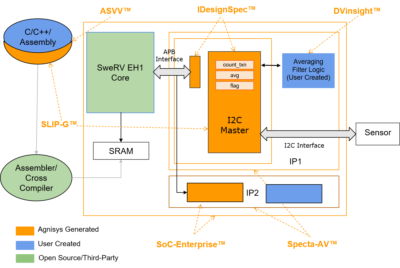
Huge designs are possible only because there is a lot of reuse from previous projects, commercial IP providers, and open-source sites. Much of this IP requires embedded software such as firmware and device drivers, one major reason why a unified development flow is so important. The entire system is developed from a specification that traditionally has been a text document. This is a challenging process since the architects must translate intent into natural language and then the designers, verification engineers, and programmers must translate natural language into silicon and code. The best way to accelerate development is to use executable specifications whenever possible so that significant amounts of hardware and software can be generated automatically. The value of this automation is even greater when the specification changes, as it does many times throughout every SoC project. There are many reasons for these changes, including new feature requirements, responses to competition, and new versions of applicable standards. In addition, trying to meet timing, area, power, testability, safety, and security goals during implementation may require specification tweaks. Every specification change has ripple effects to the hardware, software, or both. With a purely manual development flow, the designers and programmers have no choice except to make the necessary edits by hand. The embedded system must be re-verified to check out the new functionality and ensure that nothing was broken in the update process. Specification changes also ripple to the verification team, since often their environment must also be updated by hand. The system must be re-validated as well, often using emulation or FPGA prototyping. Without automation, it’s easy for the teams to get out of sync when the specification changes. Verification and validation often uncover issues due to hardware and software teams not working from same version of the specification. All this extra work consumes resources, adding to the project cost, and takes time, lengthening the time to market (TTM). Automating the design and verification process by using executable specifications has been our prime focus at Agnisys from the very beginning. From the specifications, our tools generate RTL design code, verification testbenches and tests, device drivers, documentation, and automated test equipment (ATE) programs for the fabricated chips. We automate the development of registers, memories, sequences, bus interfaces, and several types of IP. We also provide tools to connect all these elements and user-developed blocks into the complete SoC. This saves time and resources during initial development and pays dividends throughout the project. Specification changes are automatically reflected in the re-generated hardware, software, testbench, and documentation, ensuring that teams will stay in sync. We’re proud of our suite of products, and we’ve also defined a unified development flow for embedded systems that ties them all together. We provide a methodology and guidelines for how and when to use each tool for maximum value. We have worked with leading customers to understand their needs and create a flow that meets their requirements. In addition, we have created our own small SoC design to show potential users how the tools and flow work on a real project. The design averages sensor data received over an I2C interface. Sensor values are read in and converted into an averaged value by user application logic, all under control of software running on a CPU. The diagram below shows our SoC design and where our tools were used in the flow. The CPU is the open-source SweRV Core EH1, a 32-bit, 2-way superscalar, 9-stage pipeline implementation of the RISC-V architecture. Other than this core and the averaging RTL and software, the entire project was automated using our unified flow:
Automatic SoC Verification and Validation (ASVV™) generated a synchronized C-UVM verification environment and the embedded C code to verify the CSRs We have recorded a webinar with much more detail on our unified embedded development flow and how our tools are used within the flow, including the results for our example SoC design. I highly recommend that you register for the webinar here. I’m certain that you will be pleased with our latest innovation and I hope that you will use it for your next SoC project. |
|
|
|||||
|
|
|||||
|
|||||


