


Agnisys Automation Review Anupam Bakshi
Anupam Bakshi is Chief Executive Officer (CEO) for Agnisys, Inc., the pioneer and industry leader in Golden Executable Specification Solutions™. From his early days at Gateway Design Automation, through to his time at Cadence, PictureTel, and Avid Technology, he has been passionate about … More » The Role of the Portable Stimulus Standard in VLSI DevelopmentApril 23rd, 2024 by Anupam Bakshi
Semiconductor chip and intellectual property (IP) development is in a constant state of change. For architects, paper specifications have largely been replaced by abstract, executable models. Designers migrated from polygons to gates to register transfer level (RTL) descriptions. Advanced programming languages have almost entirely replaced assembly code for embedded programmers. Verification and validation engineers have seen a dramatic shift from hand-written tests to constrained-random testbenches. The portable stimulus standard (PSS) is the next step in this evolution. Introduction to PSSThe Accellera Systems Initiative, which has developed many design and verification standards, debuted PSS in 2018. The latest version is PSS 2.1, released in 2022. This relatively new standard tackled two key verification and validation challenges not well addressed by the Universal Verification Methodology (UVM), the prevailing approach for both chip and IP development:
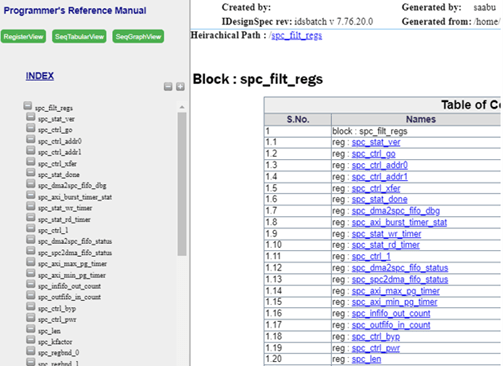
The goal of PSS was to define an abstract representation of verification (and validation) intent from which tools generate tests for the target level of the design and the target platform. It is really not the stimulus that is portable; it is the portable PSS model that enables generation of stimulus, results checking, and coverage metrics tuned for each target. For example, UVM tests are generated for simulation but not for the bringup lab, where tests are driven entirely by embedded code. 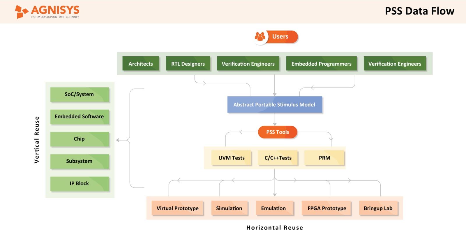 PSS Capabilities Overview Using PSS in IP and SoC DevelopmentThe scope of PSS is broad, potentially providing the ability to generate all the tests needed for verification, pre-silicon validation, and post-silicon validation. As with many aspects of engineering, one way for a smooth migration is to adopt new technologies incrementally. An excellent place to start with PSS is creating models for the addressable registers in the design. Registers are used by system drivers and embedded software to configure the design, control its operation, and gather status or results. They are part of the hardware-software interface (HSI) of every modern design. PSS 2.1 provides a solution with constructs for defining in an abstract and portable way both registers and the sequences that program them. EDA tools can generate tests specifically for each level of hierarchy and each platform, ensuring that they are all in agreement. This process usually starts at the IP level, where the architects or designers define the registers and then the verification engineers define the sequences and generate standalone tests. Engineers working on higher levels of the design hierarchy can generate appropriate tests at the push of a button. The PSS approach completely replaces the traditional approach, in which the chip-level verification team struggles to reuse standalone IP tests and the embedded programmers must manually recreate the same sequences and tests in C/C++. It is quite likely that these different sequences will not match entirely, requiring a lot of time to debug issues found during verification and validation. Generating tests with PSS ensures consistency, saves engineering resources, and shrinks the project schedule. These benefits happen not just once, but every time that register or sequence specifications change. 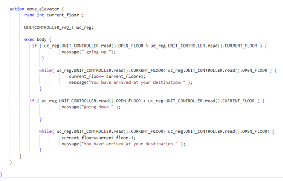 Example of PSS Code (Source: Agnisys) Making PSS Easy to UseGenerating register tests from PSS sequences is just one example of specification automation, an innovative IP and SoC development technology pioneered by the Agnisys IDesignSpec Suite. For more than fifteen years, the tools in this suite have read executable golden specifications and automatically generated a wide variety of files for design, verification, programming, validation, and documentation. This solution now supports PSS for register, memory, and sequence specification, including an intuitive and powerful PSS editor built on the popular Visual Studio (VS) Code platform. In addition to PSS, the IDesignSpec Suite supports many other input formats such as SystemRDL, IP-XACT, and spreadsheets. It can generate PSS outputs when these other formats are used for the golden specifications. Users can automatically generate both SystemVerilog/UVM and C/C++ tests from PSS models and merge these with tests generated from other input formats. Therefore, there is no need to convert existing register and sequence specifications to PSS manually in order to interact with other PSS-based verification and validation tools. The suite also generates a Programmer’s Reference Manual (PRM) that provides comprehensive documentation for programmers, developers, and end users seeking a detailed understanding of the IP or SoC design. Users can generate the PRM interactively from within the graphical design interface or via a command line in batch scripts. The PRM includes three very useful views:
 Example of PRM Register View (Source: Agnisys) 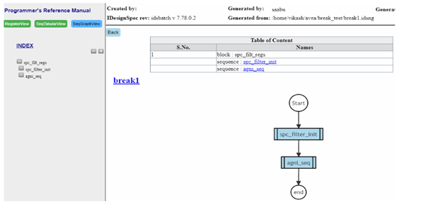 FlowChart view 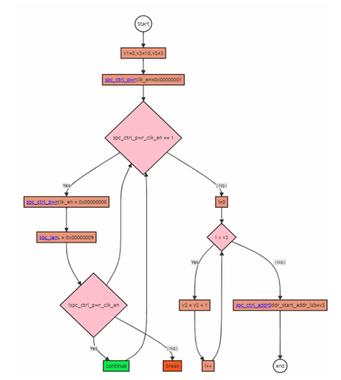 Sequence View ConclusionPSS is an important emerging method for specifying verification intent in an abstract way. Agnisys has added support for the standard alongside many other formats. This allows users to interact with PSS solutions from other vendors and to leverage PSS models provided with design IP. The Agnisys solution goes beyond other PSS-based tools by generating the RTL register design and PRM in addition to the C/C++ code, UVM tests, and testbenches required for verification and validation. This form of specification automation benefits all the teams on any IP or SoC project. Why DIY? Take Advantage of the Best Register Automation SolutionJanuary 11th, 2024 by Anupam Bakshi
Specification automation means the automatic generation of RTL design, verification, software, validation, and documentation files from executable specifications. That’s what we enable with our solutions at Agnisys. Specification automation begins with register automation. I mean that historically: registers were the first aspect of design that we tackled, and we were true pioneers of this technology. But it’s still true today: nearly everyone who takes advantage of our specification automation solutions starts with registers. Registers: The Fundamental ElementAs discussed in a recent post, registers are some of the most common and fundamental design elements. Literally everyone on a chip or intellectual property (IP) project can benefit from register automation. Your designs may contain hundreds of thousands of registers, and designing these by hand is clearly a painful task. Just typing in the register-transfer-level or RTL design code requires weeks or months of work. Like any hard coding, it’s highly susceptible to human error. Especially with many similarly named registers, typos are certain to occur. Read the rest of Why DIY? Take Advantage of the Best Register Automation Solution Specifying Registers and Sequences with Portable StimulusNovember 6th, 2023 by Anupam Bakshi
One of the most important things we do here at Agnisys is talk frequently to our users to keep track of what’s most important in the semiconductor industry. Technology is evolving constantly, industry alliances shift all the time, and the only thing constant is change. We use what we learn to make many key decisions on developing new products, adding new features to existing products, and to develop comprehensive solutions for specific user groups and vertical markets. For example, as discussed in a recent post, we found that SystemRDL is less widely adopted than IP-XCAT and so smooth translation from one to the other is a key capability that we offer. Portable Stimulus is on the RiseMore recently, we have seen a significant uptick of interest in the Portable Stimulus Standard (PSS) developed by Accellera. The first version was released in June 2018, and PSS 2.1 was announced just a few weeks ago. Key electronic design automation (EDA) companies and semiconductor developers continue to work on evolving the standard and educating engineers on how to use it successfully on real-work projects. Agnisys is proud to be a member of the PSS working group and one of several established EDA vendors with products supporting the standard. One way to view PSS is as the next step beyond the Universal Verification Methodology (UVM), which was also developed as a standard by Accellera. UVM made it much easier to reuse intellectual property (IP) designs between projects without having to rework the entire verification environment (testbench and tests). However, UVM focuses purely on SystemVerilog-based simulation and is not applicable to other verification and validation platforms. It also provides limited support across multiple levels of hierarchy, such as leveraging standalone IP testbenches at the subsystem or full-chip level. PSS was created to address both these limitations. It enables the specification of verification intent and the automatic generation of tests that work “vertically” from block to system and “horizontally” from simulation to silicon. Figure 1 is a graphical view of this portability developed by Accellera. EDA tools read an abstract PSS model and generate tests for the selected level of hierarchy and target platform. These tests can be in multiple languages and formats. For example, SystemVerilog tests run in UVM testbenches and C/C++ tests run in simulation as well as on actual silicon in the bringup lab. 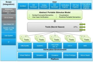 Figure 1: Accellera view of portable stimulus Read the rest of Specifying Registers and Sequences with Portable Stimulus Taking Stock of the Past YearJanuary 3rd, 2023 by Anupam Bakshi
As we transition into 2023, it’s a good time to look back over the past year and assess it, much as I did a year ago. Of course, every year has high and low points, but I have to say that 2022 was really positive for Agnisys. For one thing, in-person industry conventions returned in force, some for the first time in several years. The biggest event, as usual, was the Design Automation Conference (DAC) in San Francisco. It was back in a traditional summer slot and was quite well attended. DAC is always fun since we get to see many old friends and meet with customers. Especially with curtailed business travel in recent times, we haven’t had much face-to-face interaction. Video conferences are very helpful, but they’re not a true substitute for meeting in person. It’s also nice to be able to demonstrate our latest tools and technology live, in the interactive setting of a trade show booth, with our experts on hand to answer your questions. Automating UVM-Based IP and SoC Functional VerificationJune 22nd, 2022 by Anupam Bakshi
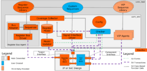
Ask a bunch of engineers about the Universal Verification Methodology (UVM) and you’ll hear two distinct sets of responses, sometimes from the same people. Most verification engineers agree that UVM was a huge leap in testbench sophistication and a boon for system-on-chip (SoC) and intellectual property (IP) development. It brought object-oriented programming (OOP), constrained-random stimulus generation, reusable verification IP (VIP), testbench automation, functional coverage, and assertions to mainstream verification users. It was developed as a standard, first by Accellera and then by the IEEE, encouraging a wide range of electronic design automation (EDA) vendors and tools to support it. UVM’s impact on the industry cannot be overestimated. Along with this praise, you’ll hear numerous reservations about UVM. Some are based on technical preferences, such as arguments that the methodology relies too much on SystemVerilog macros or that it doesn’t have enough support for aspect-oriented programming (AOP). UVM doesn’t do much to automate the manual effort of translating designer intent into verification code. UVM also has limitations on “vertical” VIP reuse from block to subsystem to SoC, which was one of the motivations for the development of the Portable Stimulus Standard (PSS). But the most common complaint you’ll hear is that UVM is difficult to learn and therefore challenging to deploy across a large verification team. Qualified UVM experts are hard to find and expensive to hire because they’re in such high demand. Even experienced UVM verification engineers say that it’s hard to remember all the details of the standard and time-consuming to develop testbenches and tests. At Agnisys, we heard these comments from our users all the time, and early in our product development effort we strove to automate the verification process as well as the design process. We started by automatically generating the register-transfer-level (RTL) design code for IP/SoC registers from an executable specification, and we quickly realized that we could do a lot to help the functional verification process as well. We could generate the UVM testbenches, and the test sequences, needed to verify the registers. We found that some users wanted to be able to execute custom programming sequences, so we added the ability to specify them in an executable format and translate them into UVM testbench sequences. Today, we support custom checks in the testbenches as well, also generated from executable specifications. In addition to the registers themselves, we also generate wrapper modules to facilitate read and write access. We provide support for access via numerous standard buses, including AXI, AHB, APB, and Avalon. In response to user demand, we added support for many special types of registers, along with appropriate UVM sequences to verify their functionality. We saw an increasing interest in using assertions both for formal verification and for providing checks in the UVM testbenches, so we also automatically generate SystemVerilog Assertions (SVA) for the registers. Our users asked us to provide RTL for standard interfaces and functions, so we introduced our library of customizable and configurable IP blocks. We generate UVM testbenches, tests, and assertions to verify the IP. The figure below does a nice job of showing all the verification-related components that we provide, every one of which replaces considerable manual effort and schedule time.
It would take a big white paper, or perhaps even a small book, to describe everything in this diagram and how we automate the process of developing it. For now, here’s a short summary of the design and UVM components that we generate automatically from executable specifications:
We should also note that design specifications change many times over the course of an IP or SoC project, and manually keeping a UVM testbench and tests updated and synchronized with the design is a huge challenge. Everything that we generate can be re-generated at the push of a button, reaping time and resource savings again and again. We generate C/C++ code for embedded programming and high-quality documentation as well. With this high level of automation, a project needs far fewer UVM experts. Verification engineers new to UVM can learn from our generated code and even the experts shorten their schedules because they do less manual work. In this post, we’ve only scratched the surface of the UVM automation capabilities in our IDS-NG™ solution. To find out more, we recommend watching our recent webinar “A Complete Automated UVM-Based Verification System” by registering here. We also invite you to visit us in our booth at the Design Automation Conference (DAC) in San Francisco in July. We’re excited to show you all the great things we can do to make your IP and SoC design and verification faster, easier, and better. Anupam Bakshi What’s New and What’s Next in Specification Automation?April 25th, 2022 by Anupam Bakshi
Over the last few months, I’ve primarily shared two kinds of posts on this blog. The Design Automation Conference (DAC) in December and the transition to the New Year prompted me to look back at how much Agnisys has expanded the power and reach of specification automation, a domain that we pioneered more than a decade ago with our register automation solutions. We have found that there are many parts of a system-on-chip (SoC) design that are amenable to automatic generation of hardware, software, testbenches, tests, and documentation from executable specifications. Of course, we’re never standing still and so I’ve also written posts covering new products and features as we’ve made them available to customers. In some cases, I’ve passed on exciting news such as last month’s announcement that our complete IDesignSpec™ Suite has been certified as compliant to the ISO 26262 and IEC 61508 functional safety standards. I find that this blog is an informal and convenient way to share information I think users will find interesting, and I hope that you feel the same. Agnisys – Certified Safe for ISO 26262 DesignApril 7th, 2022 by Anupam Bakshi
Agnisys has customers designing all sorts of intellectual property (IP) blocks, application-specific integrated circuits (ASICs), field-programmable gate arrays (FPGAs), and system-on-chip (SoC) devices across a wide range of industries worldwide. We provide specification automation solutions for registers, sequences, testbenches, assertions, standard IP, block interconnection, documentation, and more. Every chip needs these elements, and every chip can benefit from our products. However, designs for certain applications have additional requirements that are also amenable to specification automation. Safety-critical designs are a prominent example. There are many applications in which a chip failure could lead to catastrophic results. At a minimum, these designs should detect that something has gone wrong and take a safe course of action. If possible, they should continue to operate normally even after a fault occurs. This is especially important for applications such as satellites where repair or replacement of a failed component is difficult or impossible. It’s easy to think of cases in which safe operation in the presence of a fault is critical, including:
For this post, I’d like to focus on road vehicles, especially automobiles. This is the safety-critical application with which everyday users have the most contact. Cars are a particularly challenging environment for electronics, with constant vibration and regular exposure to temperature and humidity extremes. Aging chips can fail, solder joints can break, cables can disconnect, alpha particles can flip memory bits—there’s no shortage of things that can go wrong. Accordingly, in 2011 the industry created a standard to guide the functionally safe design of electrical and electronic systems in road vehicles: ISO 26262. Read the rest of Agnisys – Certified Safe for ISO 26262 Design Expanding the Scope of Specification AutomationMarch 12th, 2022 by Anupam Bakshi
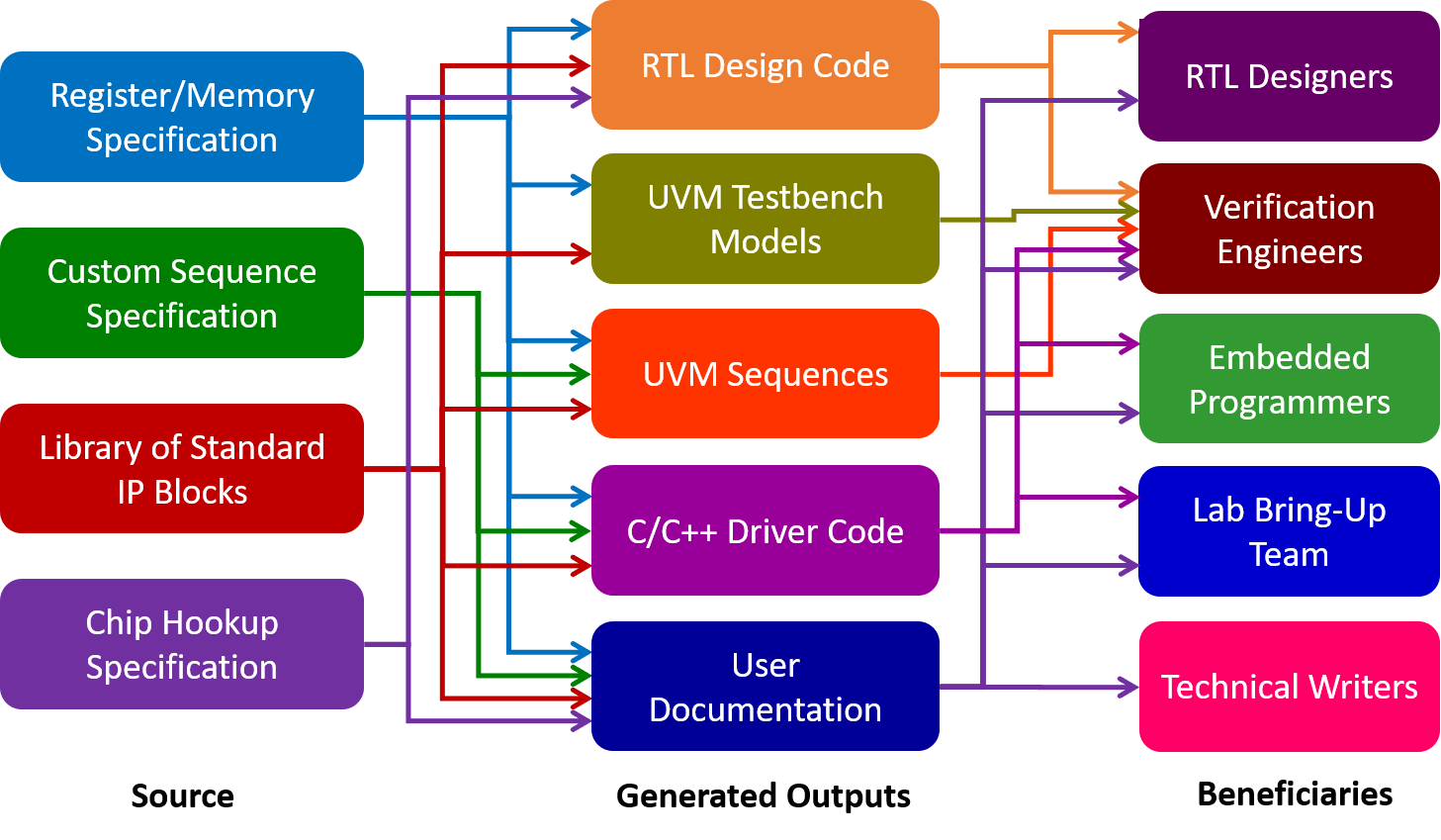
Late last year, I published a blog post that summarized what had transpired for Agnisys over the course of 2021. That was an occasion to think about how much our company and our products have expanded over time. A few weeks ago, as we prepared material for the virtual DVCon event, I again considered how much has changed for our customers and for us over the last few months. I also recalled that it was only about a year ago when we took a high-level view of our overall solution and published the following diagram in one of my posts:
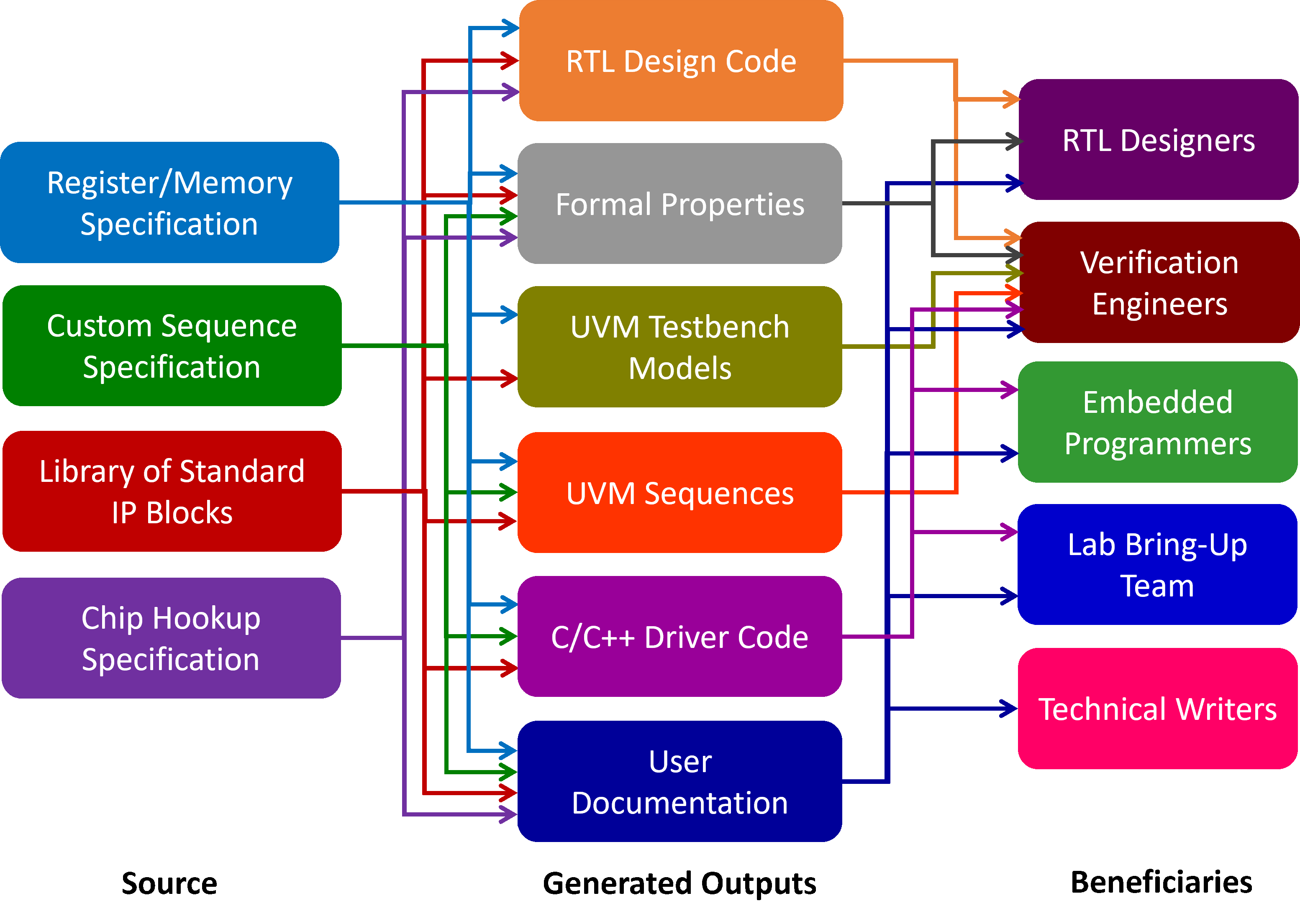
For the first time, we captured a complete view of our solution for specification-driven automation. The key is capturing as much of a system-on-chip (SoC) or IP specification as possible in executable formats and then generating as much as possible from these specifications automatically. This saves a lot of schedule time and manual effort in the early stages of a project and continues to save even more every time the specification changes. This diagram shows executable specifications for registers and memories, custom sequences, and SoC-level connections, plus a library of IP for standard functions and interfaces. Specification Automation for Embedded ProgrammersJanuary 31st, 2022 by Anupam Bakshi
As an electronic design automation (EDA) company, Agnisys provides many benefits for chip design and verification engineers. Our specification automation solution generates both the register transfer level (RTL) design and key elements for verification with simulation and formal tools. As the diagram below shows, our solution also provides value to other teams. In this post, I’d like to focus specifically on embedded programmers, since we are seeing increasing interest in our capabilities in this domain.
By embedded programming, I mean just about any type of software that interacts directly with the hardware. This includes boot code, firmware, device drivers, and what is sometimes called hardware-dependent software (HdS). In a system-on-chip (SoC) device, these programs generally run on the embedded processors within the chip, but some parts may run on a host system as well. The key common element is that the software controls and communicates with the hardware by reading and writing a set of control and status registers (CSRs). Because we support register automation, we can facilitate embedded code development by generating the C/C++ header files for the registers in the design. Winding Up an Eventful YearDecember 31st, 2021 by Anupam Bakshi
As we close in on the final days of 2021, I can’t help but think back over the events of the year and offer a few observations. At the front of my mind is the recent Design Automation Conference (DAC) in San Francisco. It was at an unusual time—December rather than June or July—and it was certainly not back to the full-scale show we all remember from the past. Some exhibitors pulled out due to pandemic-driven travel restrictions, and staffing at some booths was lower than usual. Nevertheless, it was still a very good show for Agnisys. It was great to see users in person again and to discuss their latest chip design and verification challenges. It was also nice to be able to show them our latest tools and technologies, especially since we had a lot new to talk about. As I mentioned in my DAC preview post, we made two major announcements leading up to the show. The first was the release of IDS-FPGA, part of our IDesignSpec™ (IDS) family. IDS-FPGA is integrated with the Xilinx Vivado and Intel Quartus Prime software suites to make it easier to use our automated code and IP generators on FPGA projects. As we expected, we saw considerable interest in this new offering and enjoyed the chance to demonstrate it at our booth. |
|
|
|||||
|
|
|||||
|
|||||


 Animation, 3D Art and 3D Models")