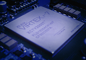
 For many years, emulators were available only to verification teams working on the largest projects in companies with deep enough pockets. Due to size rather than capabilities they were called “Big Box” emulators and typically were used in order to recover some of the time lost on RTL simulation. Meanwhile, FPGA technology has been available long enough to mature to the point where FPGA based emulation became available – and I’m not talking here about FPGA prototyping.
“Emulation – Prototyping, aren’t they just synonyms?”
Sure, they are not. The most significant differences between FPGA usage in prototypes and in emulation are shown in table 1.
|
|
Prototyping |
Emulation |
|
Clock frequency |
10-200 MHz |
1-20 MHz |
|
Clock Topology |
Multiple asynchronous sources – limited number of domains |
Derived from emulation core clock – unlimited number of domains |
|
Speed Limitation |
Fixed, |
Adaptive, |
|
Stimulus Source |
In-System, Real-world IO |
Host, |
|
Signal Capture |
Selected Nodes |
Full Visibility |
|
Memory Models |
Near-match to physical |
Modelled |
|
Design Setup |
Computer aided but with extensive user’s input and decisions |
Fully automated |
Table 1: Typical differences between FPGA usage in prototyping and emulation
FPGAs are the fastest platform for prototyping, but we can also harness that speed into our verification environment, then we can achieve runtime performance 2x to 5x faster than traditional “big box” emulation systems, and all at a fraction of the cost per gate per MHz.
“FPGAs are way too small for our SoC design, aren’t they?”
In the HES-US-2640 board, Aldec already has the largest capacity single FPGA boards commercially available today. Connecting 4 such boards in a backplane gives you 24 largest Xilinx UltraScale chips in which you can implement 633 Million ASIC Gates and still have 40% of capacity margin to facilitate FPGA Place & Route.
Figure 1: Scalable HES platform for prototyping & emulation
Not all designs need such excessive capacity, especially IoT projects, where the primary requirement is small footprint and energy-safe design. You will find the proper configuration in Aldec HES boards versatile portfolio containing Virtex-7, Virtex UltraScale and Kintex UltraScale based hardware.
For the rest of this article, visit the Aldec Design and Verification Blog.
Editor’s Note: Filling in for Bob Smith, executive director of the ESD Alliance, is Paul Cohen, its member of the technical staff.
Two upcoming events co-hosted by the ESD Alliance, “Empowering Leadership with WIT and WISDOM” and “Artificial Intelligence and Convolution Neural Networks,” are only days apart from one another and seem to tackle decidedly different topics. Or do they?
For “Empowering Leadership with WIT (Women in Technology) and WISDOM,” a panel of executives from the technology sector will explore various career choices for men and women Tuesday, November 28, at SEMI in Milpitas, Calif.
“Artificial Intelligence and Convolution Neural Networks” Monday, December 4, at San Jose State University (SJSU) will feature a panel discussion on the systems companies are building to gather data and process it to drive business operations.


