Building a Successful Non Volatile Memory (NVM) Company on the basis of CMOS Oxide Breakdown
February 27th, 2012 by Graham Bell
The following article is by Ms. Linh Hong, vice president of marketing at Kilopass Technology, Santa Clara, CA, and first appeared in the Jan. 9 issue of EDA Weekly.
Starting its second decade in business under current CEO Charlie Cheng, Kilopass Technology Inc. continues its successful growth driven by two major movements. The first comprises market forces where consumers are demanding greater functionality from their mobile smart devices beyond audio and video to include environmental data that will eventually provide life care for the consumer. The second involves technology forces that continue to deliver more transistors per silicon area for each new semiconductor process generation, now at 28nm going to 20nm.
The widespread adoption of Kilopass’ unique standard logic CMOS anti-fuse, one-time programmable (OTP), non-volatile memory (NVM) intellectual property (IP) is reflected in the growing number of Kilopass foundry and IDM partners. Among foundries signing new agreements are UMC, SMIC, GLOBALFOUNDRIES, Dongbu and TowerJazz, that join long-standing Kilopass partner TSMC, the first to offer Kilopass IP at 28nm. The key to success for an IP company is silicon enablement and Kilopass IP is available on process nodes from 180nm down to 28nm at its major foundry partners to provide solutions to customers across many markets. Among major Integrated Device Manufacturers (IDMs) inking deals with Kilopass are the major suppliers of image sensors, display drivers, and gaming chips.
To understand how this successful start-up is being driven by evolutionary technical and market forces, an explanation of the company’s patented anti-fuse NVM IP and how it compares with alternative NVM solutions is the place to begin. Next, a description of how this anti-fuse NVM IP has symbiotically evolved with the steady progression of each new generation of standard logic CMOS processes, currently at 28nm and moving to 20nm and beyond, is in order. Finally, a discussion of how the anti-fuse NVM IP uniquely serves the four high-volume applications where it is being incorporated will detail how market forces are driving the company’s ongoing success.
OTP anti-fuse memory technology has been in the available for several decades. The principle behind its operation is simple. The basic storage element is a CMOS transistor that in an un-programmed state represents an open circuit. See Figure 1. During programming, the gate oxide of the transistor is broken down to produce a low-impedance path to current flow, thus storing a bit of data. The gate oxide breakdown is permanent and is unaffected by the number of accesses, as some other NVM solutions are, or environmental factors including such hostile environments as automotive and military/aerospace.
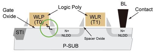
Figure 1. Kilopass 2T Bit Cell
Kilopass was founded by prolific inventor Jack Peng, who patented the technology in 2001 and contributed to early adoption of the technology by major customers. He served as company CEO until the fall of 2005, when the reins were given to serial entrepreneur Bernie Aronson. Aronson expanded the company’s customer base to over 50 and increased the number of total licenses to over a 100 all contributing to over a 100M units in chip production. After this successful run, Aronson handed the reins over to Charlie Cheng in Fall 2008. In just over a year at the end of 2010, Cheng had doubled the number of customers to 100, achieved a 100 percent revenue growth, and saw the number of chips shipped with Kilopass IP exceeding 2 billion units.
Charlie Cheng is a Silicon Valley veteran that honed his entrepreneurial skills at start-up such as Aspec Technology, Edge Computer, Iomega, Viewlogic, and Zycad. His first solo entrepreneurial venture began at Lexra, a CPU IP start-up that pioneered the first synthesizable 32-bit CPU core. After selling Lexra to MIPS Technology Inc., he joined Faraday Technology, where he held general management and marketing vice president roles before taking the helm as Chief Executive Officer. After four years he left to become Entrepreneur-in-Residence at U.S. Venture Partners, a major Kilopass Technology investor, with the eye to finding a start-up he where he could employ the full weight of his accumulated experience. Kilopass provided the ideal vehicle. Fluent in both English and Mandarin Chinese, Cheng is a graduate of Cornell University with a degree in mechanical engineering and computer science.
Making a Standard Logic CMOS Anti-Fuse
Peng’s invention enabled Kilopass to implement an anti-fuse in standard CMOS without additional mask or process steps—no extra cost—and to allow an elevated programming voltage to convert a standard CMOS transistor into a low-resistance path to current: an anti fuse or bit cell. Until 2001, When Kilopass was formed, to create the memory element or bit cell required additional process steps. Kilopass was conceived when 180nm standard logic CMOS process technology became the volume manufacturing process for the semiconductor industry. At this process node, the gate oxide breakdown is less than that of the junction breakdown, thus eliminating the need for added manufacturing steps. Previously, extra protection had to be added to the transistor to prevent junction breakdown—the destruction of the transistor. This extra protection added manufacturing steps, thus boosting the cost adding anti-fuse capability to any chip.
With each new CMOS process generation, transistor dimensions and the oxide thickness get smaller. This shrinking makes the anti-fuse solution better because the programming voltage required to cause gate oxide breakdown is reduced. The process scaling also provides other benefits. The most obvious is smaller transistors allow more memory to be contained in a given silicon area. Furthermore, successively smaller memory cell make the Kilopass memory, which is the most tamper-resistant NVM available, more secure. The extra security results from the smaller read currents needed to access data from any bit cell.
Kilopass has 59 patents that have been issued or pending on anti-fuse technology. As shown in figure 2, the patents are divided into three groups of fundamental bit cells by number of transistors – 1T, 2T, and 3.5T. Kilopass’ patents enable the embedding of OTP macros in standard CMOS products:
- 42 are issued, 17 pending in United States, China, Taiwan, Japan, and EPC.
- 21 Issued in United States for 1T, 2T, and 3.5T anti-fuse bit cell technologies.
- 5 for 1T, 15 for 2T, and 1 for 3.5T
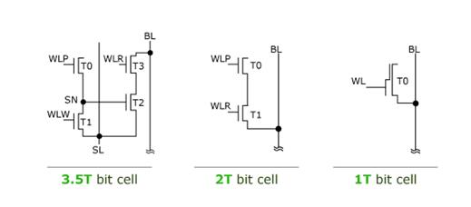 Figure 2. Anti-Fuse Patent Portfolio
Comparing NVM Alternatives
The competitive advantage of anti-fuse is best illustrated by comparing it with other embedded NVM technologies available in the market:
- Embedded Flash solutions where data is represented as a charge;
- Floating gate or charge trapping solutions that likewise represent data as a charge;
- Electrical fuse solutions that blow a metal link or the silicide on a poly line to represent data as a change in resistance;
- Via or diffusion ROM that represent data as a short or open at a given node in a memory array fabricated in the metal layer of a chip during manufacture.
Embedded Flash, the most expensive and most flexible of the embedded NVM technologies, is ideal for code and data storage that changes often. It can require at least 10 additional mask steps. The higher upfront cost of the technology is offset by high endurance allowing frequent and a large number of read-write cycles. Commonly found in microcontrollers (MCU) it provides flexibility to end applications to produce multiple configurations from one product.
For example, an MCU chip manufacturer may produce a low end 8-bit MCU for a dozen different appliance manufacturers. By producing a base MCU and adding different features for each of the different customers in flash, the MCU supplier eliminates the need to manufacture a different MCU for each customer—thus saving silicon cost and eliminating the inventory problem of stockpiling different products for different customers. Both the vendor and the customer benefit from the flexibility, respectively, to control inventory and provide differentiation.
An alternative to flash is floating gate or charge trapping solutions in the form of the stacked-gate 1T cell, a CMOS transistor with one floating gate and one contacted gate overlapping each other. See Figure 3. Insulated by a high quality oxide from the contacted gate, the floating gate is programmed by channel injecting electrons and erased by allowing the trapped electrons to escape. The presence or absence of electrons in the floating gate is read as a “1” or “0”. Like flash the floating gate memory can be erased and electrically programmed.
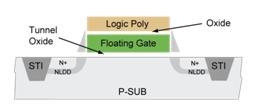 Figure 3. Floating Gate NVM Technology
However, both flash and the floating gate solution requires additional masks and processing steps on top of the standard CMOS logic process though the latter requires fewer than former. How much additional cost a design requiring an embedded re-programmable NVM can bear will determine if an application will opt for the flash or floating gate alternative. Having to add processing steps to the standard logic CMOS process means that these two solutions will not be available at the latest process node. Typically flash on logic CMOS will lag standard logic CMOS three generations whereas floating gate may be one or two generations behind.
Another alternative NVM storage technology is electrical fuse (eFuse) made of polysilicon or metals. The metal eFuse is a one-time programmable memory programmed by applying a high current to rupture a conductive link or make its resistance significantly higher. The reliability of an eFuse is a concern because debris and shards can cause the fuse to grow back over time. See figure 4. The polysilicon eFuse with Cobalt or Nickel silicide on top is programmed by a well-known reliability mechanism called electro-migration in which electron momentum pushes the silicide atoms out of the conductor link to produce a high resistance or open circuit.

Figure 4. Poly Fuse Technology
The eFuse is typically custom-designed and provided by the foundry as a macro, thus affording the designer a lower cost solution. However, migrating a design containing an eFuse from one foundry to another becomes problematic. Most fuses are programmed during wafer fabrication with stringent power requirements for programming. The eFuse bit cell is the largest of the standard CMOS NVM technologies. If an application calls for higher bit density, greater than 4Kb, another 4Kb eFuse increment begins to take up too much area of the SOC.
Finally, among all the NVM alternatives, ROM is the lowest cost technology available, however, it is the least flexible of all. ROM is typically used for storing code that does not change such as audio recording of “Happy Birthday” in a musical greeting card or fonts in an ink jet printer. The ROM is programmed as part of wafer fabrication, thus, the content can only be changed by producing a new mask layer.
The anti-fuse NVM addresses all the shortcomings of the four alternative NVM solutions. Unlike flash or other charge trapping NVM solutions, anti-fuse requires no additional cost over standard CMOS and scales easily with each new generation of process technology. Unlike the eFuse and ROM solutions, anti-fuse can be programmed in the final package in the field with a simple write command. And, unlike eFuse and ROM, anti-fuse is portable across multiple foundries and multiple processes from 180nm to 28nm. Finally, of all the NVM solutions anti-fuse is the most tamper-resistant, even to invasive attacks and scanning electron microscope observation.
Growing Demand for Embedded NVM
Fueling the company’s success and growth is the increasing consumption of digital multimedia content on portable devices—smart-phones and tablets and consumer electronics devices in the home—Internet TVs and web-enabled set-top boxes. Further demand for the company’s NVM intellectual property (IP) is coming from being incorporated in microcontrollers (MCU) targeting automotive applications. Over a hundred MCU’s provide control of engine, transmission power, auto body, cabin environment, lamp, security, and audio entertainment in a typical new car today. Finally, the number of analog and mixed signal circuits being incorporated on next generation system on chip (SoC) designs continues to grow producing additional consumption of Kilopass NVM IP
According to a Global Industry Analysts, Inc. market research report published in May of 2011, the global smart phones market will reach over 1.6 Billion units by 2017. This growth is being fueled by a plethora of functionality smart phones provide such as data services: applications, multimedia, location-based services. The market research firm sees near-field communications that enable wireless purchases, electronic wallet, etc. becoming prevalent in the next generation of devices. All this functionality is fertile ground for theft and fraud by hackers exploiting the technology. NVM memory within these portable devices provides tamper-resistant storage for personal identification numbers (PINs), encryption keys, and other private information. However most NVM technology is relatively easy to hack.
Kilopass’ embedded non-volatile memory cannot be hacked using passive, semi-invasive, and invasive methods. Due to the nature of the technology, it is difficult to determine the content of the memory. Passive techniques including using current profiles to determine the word pattern are unsuccessful because the bit cell current for “0”s and “1”s are much smaller than the current required for sensing or to operate the peripheral circuits in order to read the memory. One cannot determine the pattern of the word being read. Invasive techniques including backside attacks or scanning electron microscope passive voltage contrast are unsuccessful because it is very difficult to isolate the bit cell since it is connected in a cross point array. Furthermore, it is difficult using chemical etching or mechanical polishing to locate the oxide breakdown. In a cross-section or a top view, it is difficult to determine which bit is programmed.

Figure 5. NVM in Smart Phones
Figure 5 shows typical functions contained in a smart phone. All can achieves higher integration by using embedded nonvolatile memory (NVM) instead of serial flash memory or EEPROM on separate die. Kilopass estimates that 30 percent of the $5 billion spent each year on serial flash memory and EEPROM was for applications requiring 4Mb of memory or less. Kilopass states that teardowns of Apple’s iPhone 3GS found about 10 serial flash memories and EEPROMs, most die-bonded within packages of larger chips thus invisible in system-level teardowns. As smart phones continue to offer more features, embedded NVM memory will become more valuable to reduce chip count and to add security.
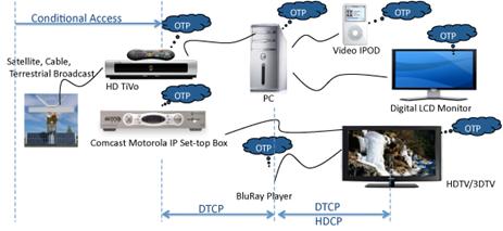
Figure 6. NVM in Home Electronics
In home consumer electronics non-volatile memory has typically been used for conditional access, the encryption key loaded into the set-top box that enables the consumer to receive content from the service provider. However, as shown in Figure 6 with the advent of over-the-top media, content is circumventing the cable and satellite gateways via the Internet and the wired and wireless home networks that connect consumer electronics with PCs and digital devices.
Over-the-top media has spawned the proliferation of digital rights management codes that accompany the digital multimedia over the Internet and throughout the home network. For example DTCP (Digital Transmission Content Protection) keys can be found on interface such as IEEE 1394, USB, MOST, Bluetooth, and TCP/IP or HDCP (High-bandwidth Digital Content Protection) keys can be found on interfaces such as HDMI, DVI, Display Port, GVIF and UDI.
NVM in Automotive Applications
For today’s premium cars, “the cost of software and electronics can reach 35 to 40 percent of the cost of a car,” said Manfred Broy, a professor of informatics at Technical University, Munich quoted in a story in IEEE Spectrum published in February 2009. The article asserted that these cars contain 70 to 100 microcontroller-based electronic control units (ECUs) networked throughout the body of your car as illustrated in Figure 7. Even low-end cars now have 30 to 50 ECUs embedded in the body, doors, dash, roof, trunk, seats, and elsewhere.
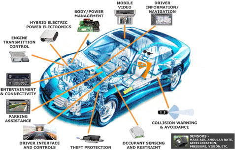
Figure 7. NVM in the Automobile
Microcontrollers (MCUs) provide the intelligence directing this electronics. With the growing awareness for the need for security, automobile manufacturers are looking for new alternative to flash and EEPROM for secure, low-cost, more temperature tolerant and often field-programmable non-volatile memory (NVM) for microcontrollers in automotive electronic systems. One-time programmable anti-fuse NVM with over-provisioned memory capacity is finding applications where storage contents changes infrequently over the life of the automobile: boot code for microcontrollers—eliminating external serial EEPROM, ROM patches to fix bugs in the field, data logging of infrequently changing events—odometer reaching service milestones, etc.
Analog mixed-signal circuits, including digital to analog converters, analog to digital converters, pulse width modulators, etc., are proliferating in new chips populated by sensors, accelerometers, and radio frequency circuits. According to a TechNavio market research report published May 2011, the global analog and mixed signal device market will reach $49.45 billion in 2014. One of the key factors contributing to this market’s growth is the explosion in intelligent handheld mobile device that are incorporating applications (apps) that enable the device to sense the environment, location, speed, direction as well as interact with the user through voice recognition and text to speech synthesis.
Chips containing these analog mixed signal elements will soon include even more sensors than the ubiquitous accelerometer and GPS. According to the article “Which sensors are coming to your next smartphone?” in the May 23, 2011 issue of web magazine Mobihealthnews.com, the following are in the offing: altimeters, heart-rate monitors as well as sensors to detect perspiration and microphones, temperature and humidity sensors for more environmental data. Each will bring their share of analog mixed-signal circuits.
The problem with analog mixed-signal circuits is they are subject to variations during manufacture and their characteristics change over time. To ensure they behave consistently, the circuits’ characteristics are trimmed during manufacture using digital parameters stored in NVM. As the analog mixed-signal circuits’ characteristics drift over time, they are trimmed by changing the parameters in NVM to compensate for the drift. Storing these parameters presents a large market opportunity for NVM IP.
Summary
Kilopass Technology Inc. is an intellectual property company that has both significant market forces and compelling technology trends driving its success. Propelling its business success is the proliferation of multimedia content in handheld devices, all requiring secure DRM key storage. Couple this with the increasing number of computing devices that all need NVM storage being incorporated into the smart devices to handle the expanding amount of functionality. And finally add in the expanding number of sensors migrating on board portable smart devices all needing NVM storage for mixed signal trimming data. The compelling technical trend driving the company forward is the relentless progression of Moore’s Law producing the next generation CMOS process technology every 18 months. With each new generation, the storage capacity of Kilopass IP grows, its reliability improves, the amount of power it consumes decreases, and its ability to thwart tampering even with the most invasive technique improves. Kilopass is well positioned for continued growth and success. End of article.

Ms. Linh Hong is VP of marketing at Kilopass responsible for marketing Kilopass’ solutions globally. With 13 years of semiconductor industry experience – primarily focused on logic NVM IP, high-speed SERDES IP and broadband communication ASICs – Linh served for three years in various director and management positions in field applications engineering and applications marketing at Kilopass before assuming her current role in April 2009. Prior to joining Kilopass, she was a design consultant and design manager at LSI Logic, where she also served in various design and marketing engineering functions. She began her career as a component engineer at Sun Microsystems. Linh holds a BS degree with honors in physics, and an MSEE degree in electrical engineering, both from University of California, Davis.
About Kilopass
Kilopass Technology is expanding the horizons of embedded non-volatile memory to create new cost savings and design opportunities for today’s semiconductor industry.
The leader in embedded NVM intellectual property, Kilopass removes long-standing challenges to NVM integration across a wide range of markets, applications and SOC designs. Its patented technologies and expanding set of one-time programmable (OTP) and multi-time programmable NVM solutions have boundless capacity to scale to advanced CMOS process geometries, are portable to every major foundry and integrated device manufacturer (IDM), and meet market demands for increased integration, higher densities, lower cost, better reliability and improved security.
Trusted by today’s most trusted brands, Kilopass technology has been integrated by over 100 customers, with more than 2 billion units shipped in over 300 industrial, automotive, consumer electronics, mobile and analog & mixed signal chip designs. The company’s solutions are currently integrated into 20 million set-top boxes, 50 million DVD chip sets, 100 million Wi-Fi modules, and 500 million FM tuners.
Related
This entry was posted
on Monday, February 27th, 2012 at 4:11 pm.
You can follow any responses to this entry through the RSS 2.0 feed.
You can leave a response, or trackback from your own site.


 Animation, 3D Art and 3D Models")
good reeding