|
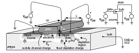
[ Chapter start ] [ Previous page ] [ Next page ] 2.1 CMOS TransistorsFigure 2.3 illustrates how electrons and holes abandon their dopant atoms leaving a depletion region around a transistor’s source and drain. The region between source and drain is normally nonconducting. To make an n -channel transistor conducting, we must apply a positive voltage V GS (the gate voltage with respect to the source) that is greater than the n -channel transistor threshold voltage , V t n (a typical value is 0.5 V and, as far as we are presently concerned, is a constant). This establishes a thin ( ª 50 Å) conducting channel of electrons under the gate. MOS transistors can carry a very small current (the subthreshold current —a few microamperes or less) with V GS < V t n , but we shall ignore this. A transistor can be conducting ( V GS > V t n ) without any current flowing. To make current flow in an n -channel transistor we must also apply a positive voltage, V DS , to the drain with respect to the source. Figure 2.3 shows these connections and the connection to the fourth terminal of an MOS transistor—the bulk ( well , tub , or substrate ) terminal. For an n -channel transistor we must connect the bulk to the most negative potential, GND or VSS, to reverse bias the bulk-to-drain and bulk-to-source pn -diodes. The arrow in the four-terminal n -channel transistor symbol in Figure 2.3 reflects the polarity of these pn -diodes. The current flowing in the transistor is
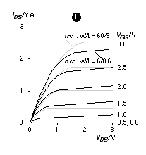
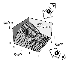
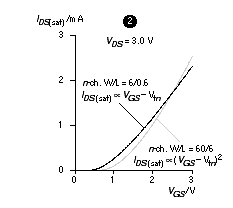
We can express the current in terms of the total charge in the channel, Q (imagine taking a picture and counting the number of electrons in the channel at that instant). If t f (for time of flight —sometimes called the transit time ) is the time that it takes an electron to cross between source and drain, the drain-to-source current, I DSn , is We need to find Q and t f . The velocity of the electrons v (a vector) is given by the equation that forms the basis of Ohm’s law: where m n is the electron mobility ( m p is the hole mobility ) and E is the electric field (with units Vm –1 ). Typical carrier mobility values are m n = 500–1000 cm 2 V –1 s –1 and m p = 100–400 cm 2 V –1 s –1 . Equation 2.3 is a vector equation, but we shall ignore the vertical electric field and concentrate on the horizontal electric field, E x , that moves the electrons between source and drain. The horizontal component of the electric field is E x = – V DS / L, directed from the drain to the source, where L is the channel length (see Figure 2.3). The electrons travel a distance L with horizontal velocity v x = – m n E x , so that Next we find the channel charge, Q . The channel and the gate form the plates of a capacitor, separated by an insulator—the gate oxide. We know that the charge on a linear capacitor, C, is Q = C V . Our lower plate, the channel, is not a linear conductor. Charge only appears on the lower plate when the voltage between the gate and the channel, V GC , exceeds the n -channel threshold voltage. For our nonlinear capacitor we need to modify the equation for a linear capacitor to the following: The lower plate of our capacitor is resistive and conducting current, so that the potential in the channel, V GC , varies. In fact, V GC = V GS at the source and V GC = V GS – V DS at the drain. What we really should do is find an expression for the channel charge as a function of channel voltage and sum (integrate) the charge all the way across the channel, from x = 0 (at the source) to x = L (at the drain). Instead we shall assume that the channel voltage, V GC ( x ), is a linear function of distance from the source and take the average value of the charge, which is thus The gate capacitance, C , is given by the formula for a parallel-plate capacitor with length L , width W , and plate separation equal to the gate-oxide thickness, T ox . Thus the gate capacitance is where e ox is the gate-oxide dielectric permittivity. For silicon dioxide, Si0 2 , e ox ª 3.45 ¥ 10 –11 Fm –1 , so that, for a typical gate-oxide thickness of 100 Å (1 Å = 1 angstrom = 0.1 nm), the gate capacitance per unit area, C ox ª 3 f F m m –2 . Now we can express the channel charge in terms of the transistor parameters, Finally, the drain–source current is The constant k ' n is the process transconductance parameter (or intrinsic transconductance ): We also define b n , the transistor gain factor (or just gain factor ) as The factor W/L (transistor width divided by length) is the transistor shape factor . Equation 2.9 describes the linear region (or triode region) of operation. This equation is valid until V DS = V GS – V t n and then predicts that I DS decreases with increasing V DS , which does not make physical sense. At V DS = V GS – V t n = V DS (sat) (the saturation voltage ) there is no longer enough voltage between the gate and the drain end of the channel to support any channel charge. Clearly a small amount of charge remains or the current would go to zero, but with very little free charge the channel resistance in a small region close to the drain increases rapidly and any further increase in V DS is dropped over this region. Thus for V DS > V GS – V t n (the saturation region , or pentode region, of operation) the drain current IDS remains approximately constant at the saturation current , I DSn (sat) , where Figure 2.4 shows the n -channel transistor I DS –V DS characteristics for a generic 0.5 m m CMOS process that we shall call G5 . We can fit Eq. 2.12 to the long-channel transistor characteristics (W = 60 m m, L = 6 m m) in Figure 2.4(a). If I DSn (sat) = 2.5 mA (with V DS = 3.0 V, V GS = 3.0 V, V t n = 0.65 V, T ox =100 Å), the intrinsic transconductance is or approximately 90 m AV –2 . This value of k ' n , calculated in the saturation region, will be different (typically lower by a factor of 2 or more) from the value of k ' n measured in the linear region. We assumed the mobility, m n , and the threshold voltage, V t n , are constants—neither of which is true, as we shall see in Section 2.1.2. For the p -channel transistor in the G5 process, I DSp (sat) = –850 m A ( V DS = –3.0 V, V GS = –3.0 V, V t p = –0.85 V, W = 60 m m, L = 6 m m). Then The next section explains the signs in Eq. 2.14. 2.1.1 P-Channel TransistorsThe source and drain of CMOS transistors look identical; we have to know which way the current is flowing to distinguish them. The source of an n -channel transistor is lower in potential than the drain and vice versa for a p -channel transistor. In an n -channel transistor the threshold voltage, V t n , is normally positive, and the terminal voltages V DS and V GS are also usually positive. In a p -channel transistor V t p is normally negative and we have a choice: We can write everything in terms of the magnitudes of the voltages and currents or we can use negative signs in a consistent fashion. Here are the equations for a p -channel transistor using negative signs:
In these two equations V t p is negative, and the terminal voltages V DS and V GS are also normally negative (and –3 V < –2 V, for example). The current I DSp is then negative, corresponding to conventional current flowing from source to drain of a p -channel transistor (and hence the negative sign for I DSp (sat) in Eq. 2.14). 2.1.2 Velocity SaturationFor a deep submicron transistor, Eq. 2.12 may overestimate the drain–source current by a factor of 2 or more. There are three reasons for this error. First, the threshold voltage is not constant. Second, the actual length of the channel (the electrical or effective length, often written as L eff ) is less than the drawn (mask) length. The third reason is that Eq. 2.3 is not valid for high electric fields. The electrons cannot move any faster than about v max n = 10 5 ms –1 when the electric field is above 10 6 Vm –1 (reached when 1 V is dropped across 1 m m); the electrons become velocity saturated . In this case t f = L eff / v max n , the drain–source saturation current is independent of the transistor length, and Eq. 2.12 becomes
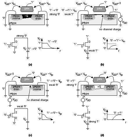
We can see this behavior for the short-channel transistor characteristics in Figure 2.4(a) and (c). Transistor current is often specified per micron of gate width because of the form of Eq. 2.16. As an example, suppose I DSn (sat) / W = 300 m A m m –1 for the n -channel transistors in our G5 process (with V DS = 3.0 V, V GS = 3.0 V, V t n = 0.65 V, L eff = 0.5 m m and T ox = 100 Å). Then E x ª (3 – 0.65) V / 0.5 m m ª 5 V m m –1 , and t f ª 0.5 m m/37,000 ms –1 ª 13 ps. The value for v max n is lower than the 10 5 ms –1 we expected because the carrier velocity is also lowered by mobility degradation due the vertical electric field—which we have ignored. This vertical field forces the carriers to keep “bumping” in to the interface between the silicon and the gate oxide, slowing them down. 2.1.3 SPICE ModelsThe simulation program SPICE (which stands for Simulation Program with Integrated Circuit Emphasis ) is often used to characterize logic cells. Table 2.1 shows a typical set of model parameters for our G5 process. The SPICE parameter KP (given in m AV –2 ) corresponds to k ' n (and k ' p ). SPICE parameters VT0 and TOX correspond to V t n (and V t p ), and T ox . SPICE parameter U0 (given in cm 2 V –1 s –1 ) corresponds to the ideal bulk mobility values, m n (and m p ). Many of the other parameters model velocity saturation and mobility degradation (and thus the effective value of k ' n and k ' p ). 2.1.4 Logic LevelsFigure 2.5 shows how to use transistors as logic switches. The bulk connection for the n -channel transistor in Figure 2.5(a–b) is a p -well. The bulk connection for the p -channel transistor is an n -well. The remaining connections show what happens when we try and pass a logic signal between the drain and source terminals.
In Figure 2.5(a) we apply a logic '1' (or VDD —I shall use these interchangeably) to the gate and a logic '0' ( V SS ) to the source (we know it is the source since electrons must flow from this point, since V SS is the lowest voltage on the chip). The application of these voltages makes the n -channel transistor conduct current, and electrons flow from source to drain. Suppose the drain is initially at logic '1'; then the n -channel transistor will begin to discharge any capacitance that is connected to its drain (due to another logic cell, for example). This will continue until the drain terminal reaches a logic '0', and at that time V GD and V GS are both equal to V DD , a full logic '1'. The transistor is strongly conducting now (with a large channel charge, Q , but there is no current flowing since V DS = 0 V). The transistor will strongly object to attempts to change its drain terminal from a logic '0'. We say that the logic level at the drain is a strong '0'. In Figure 2.5(b) we apply a logic '1' to the drain (it must now be the drain since electrons have to flow toward a logic '1'). The situation is now quite different—the transistor is still on but V GS is decreasing as the source voltage approaches its final value. In fact, the source terminal never gets to a logic '1'—the source will stop increasing in voltage when V GS reaches V t n . At this point the transistor is very nearly off and the source voltage creeps slowly up to V DD – V t n . Because the transistor is very nearly off, it would be easy for a logic cell connected to the source to change the potential there, since there is so little channel charge. The logic level at the source is a weak '1'. Figure 2.5(c–d) show the state of affairs for a p -channel transistor is the exact reverse or complement of the n -channel transistor situation. In summary, we have the following logic levels:
Sometimes we refer to the weak versions of '0' and '1' as degraded logic levels . In CMOS technology we can use both types of transistor together to produce strong '0' logic levels as well as strong '1' logic levels. [ Chapter start ] [ Previous page ] [ Next page ] | |||||||||||||||||||||||||||||||||||||||||||||||||||||||||||||||||||||||||||||||||||||||||||||||||||||||||||||||||||||||||||||||||||||||||||||||||||||||||||||||||||||||||||||||||||||||||||||||||||||||||||||||||||||||||||||
