


Siemens EDA Juergen Jaeger
Juergen Jaeger is the director of prototyping product strategy for Simens EDA. Prior to joining Siemens, Juergen was the director of product management at Cadence Design Systems, responsible for all FPGA-based prototyping activities. Prior to that he worked at Synopsys via the acquisition of … More » FPGA-Based Prototyping – from “Do-It-Yourself” to an Essential SoC Verification and System Validation ToolAugust 26th, 2024 by Juergen Jaeger
Then chip designs exploded in complexity, software content increased exponentially, and the sheer amount of data going in and out of an SoC grew by orders of magnitude. And let’s not forget that design cycles shrank at the same time. FPGA-based prototype platforms, uniquely suited to address those challenges, have become essential to SoC verification and system validation. As all this change was happening, prototyping evolved as well. Today it is no longer a construction kit, but a ready-to-use, comprehensive solution that delivers significant productivity gains. You might ask, what are the primary attributes of this evolved FPGA-based prototyping platforms? Obviously, it’s hardware consisting of one or more FPGAs! It’s also the software that takes the ASIC RTL and intelligently maps it into the collection of FPGAs. It’s also a test environment that stimulates the design, often with live system interfaces like sensors, cameras, and ethernet traffic.
So, in a nutshell, the FPGA-based prototype system is a pre-silicon digital twin of your SoC or IP design. This digital twin is now a cycle-accurate representation of your design, running fast enough to boot the firmware and the operating system and to run the actual software workloads. And that’s exactly what our Veloce proFPGA CS platform is.
Now, just like with the RTL design that is validated on our FPGA-based prototypes, which can’t do much without software, the same is true for the prototyping platform. Mapping a design into multiple FPGAs can be a cumbersome and time-consuming adventure. Therefore, equally important as the hardware itself is the software flow to compile the design:
So, the software is critical to success, and that’s where VPS (Veloce Prototyping Software) comes in.
To learn more, download the Veloce proFPGA CS factsheet or contact us at 1-800-547-3000 for details. In upcoming blogs, we take a closer look at key technical aspects, starting with how the larger gate capacity of the latest FPGAs enables new use modes. Especially in the area of automatic, multi-FPGA partitioning, debug, and at-speed interface implementation. I encourage you to check back frequently and leave comments about what’s been helpful. |
|
|
|||||
|
|
|||||
|
|||||
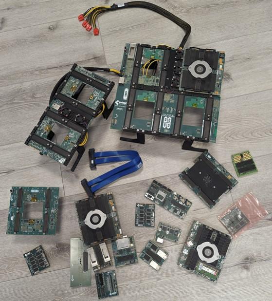 FPGA-based prototyping has always been something of an assembly-required construction kit. Consequently, getting to a functional and usable prototype took a lot of effort, time, and a ‘do it yourself’ attitude. Once up and running, however, the reward justified the effort by providing a fast pre-silicon verification platform, with frequencies often running at tens of megahertz and reducing verification workload runs from days to minutes.
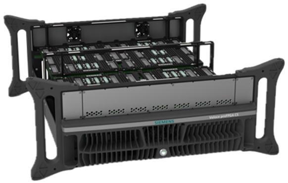 It has debug capabilities like memory backdoor access to quickly update boot images, monitor register and memory contents and validate functionality. It also lets you connect to live system interfaces to run real-world scenarios.


 Animation, 3D Art and 3D Models")