


EDACafe Editorial Roberto Frazzoli
Roberto Frazzoli is a contributing editor to EDACafe. His interests as a technology journalist focus on the semiconductor ecosystem in all its aspects. Roberto started covering electronics in 1987. His weekly contribution to EDACafe started in early 2019. The one million ARM-cores neuromorphic machineAugust 29th, 2019 by Roberto Frazzoli
Favorable wind keeps blowing for SpiNNaker, a research project led by the University of Manchester (UK) which in November 2018 reached its ambitious goal: a neuromorphic machine containing one million ARM cores, capable of simulating one billion simple neurons in biological real time. This result came after several years of development, as the SpiNNaker project – funded by the European Union – formally began in 2005, with first working silicon delivered in 2011. The second phase of the initiative, called SpiNNaker2, has already been planned, aiming to a 10x boost in performance and efficiency over the first generation. Let’s take a closer look at SpiNNaker (a contraction of Spiking Neural Network Architecture), as it is described in the project’s website and in two papers – here and here – authored by the research group, where many more details can be found. 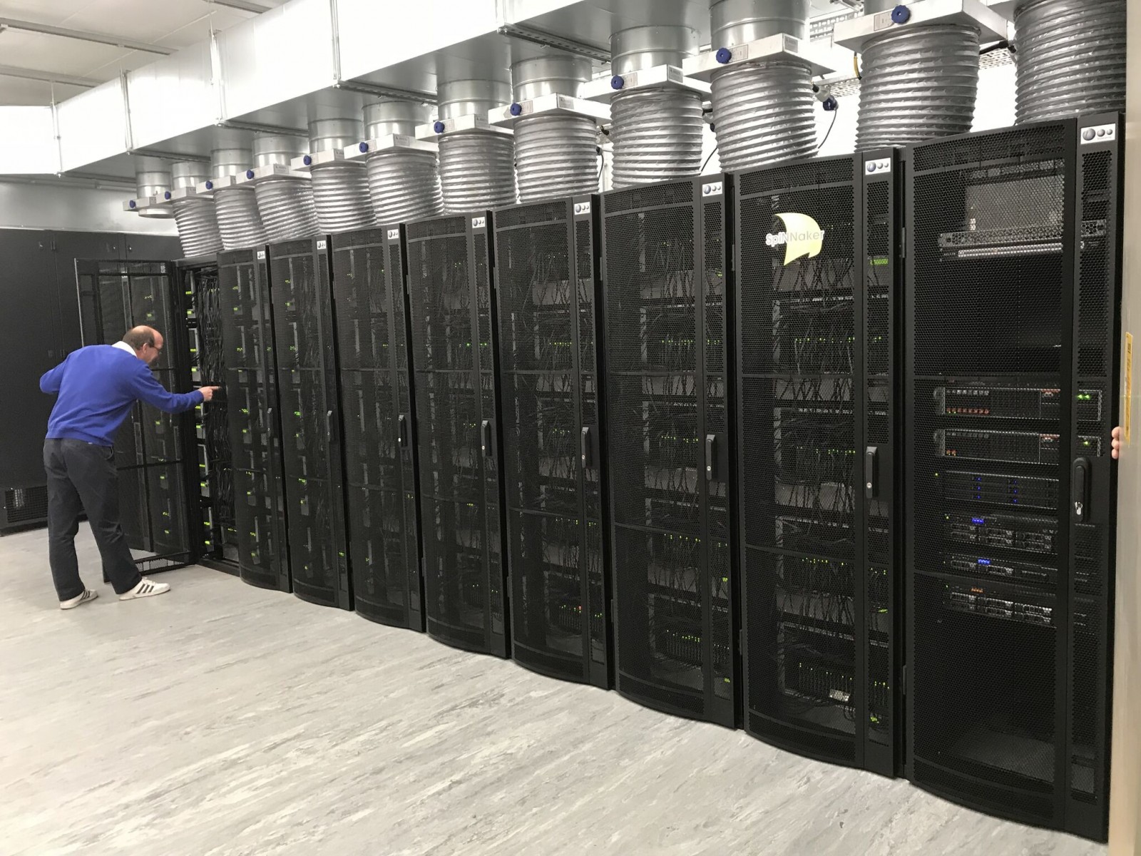 The one million ARM-cores SpiNNaker machine. Image credit: University of Manchester A novel approach to parallel computing Led by professor Steve Furber from University of Manchester’s Advanced Processor Technologies (APT) Research Group, the SpiNNaker project is based on a novel approach to parallel computing, placing special emphasis on low power consumption and fault-tolerance. As researchers explained, “SpiNNaker breaks the rules followed by traditional supercomputers that rely on deterministic, repeatable communications and reliable computation. SpiNNaker nodes communicate using simple messages (spikes) that are inherently unreliable.” (…) “Three of the principle axioms of parallel machine design – memory coherence, synchronicity and determinism – have been discarded in the design without, surprisingly, compromising the ability to perform meaningful computations.
A further attribute of the system is the acknowledgment, from the initial design stages, that the sheer size of the implementation will make component failures an inevitable aspect of day-to-day operation, and fault detection and recovery mechanisms have been built into the system at many levels of abstraction.” As an example of this, the packet switching infrastructure used by the system will drop the “outdated” packets that couldn’t be forwarded within a preset time. Dropped packets are not re-sent. According to the researchers, this emulates the behavior of biological neural networks, where the death of individual neuron cells (one per second in human brains) or signals loss do not prevent normal functioning. The emphasis on low power consumption and fault-tolerance has also directed design choices at the chip level: using energy efficient ARM9 embedded processors and Mobile DDR SDRAM, designers have sacrificed some performance for enhanced power efficiency. Also, each ARM core is tested at start-up, and can be disabled in case of fault. All cores have the same capabilities, and any specialized functions – such as system monitoring – are assigned after start-up test. Hence, even if several cores fail, the rest of the device can continue to work.  Professor Steve Furber. Image credit: University of Manchester The SpiNNaker chip The basic building block of the systems is the SpiNNaker chip, which contains eighteen ARM968 cores. Neurons are modeled in software and their spikes generate packets that propagate through the on-chip and inter-chip communication fabric, relying on custom-made on-chip multicast routers. The device is based on a Globally Asynchronous Locally Synchronous (GALS) architecture, with each core residing in its synchronous island, surrounded by a packet-switched asynchronous communications infrastructure. The packets are small (40 or 72 bits), and their transmission is brokered entirely by hardware, resulting in a bisection bandwidth of over 5 billion packets/s. Two distinct networks-on-chip are used: the system NoC, which replaces a conventional on-chip bus for the system interconnect; and the communications NoC, providing the on-chip and off-chip packet switching infrastructure. Both NoCs are based on Chain, a delay-insensitive communication technology developed at the University of Manchester. Each node in the SpiNNaker system architecture is a System-in-Package containing two silicon dies: the above-described chip, and a 128 MByte SDRAM die which is physically mounted on top of it. 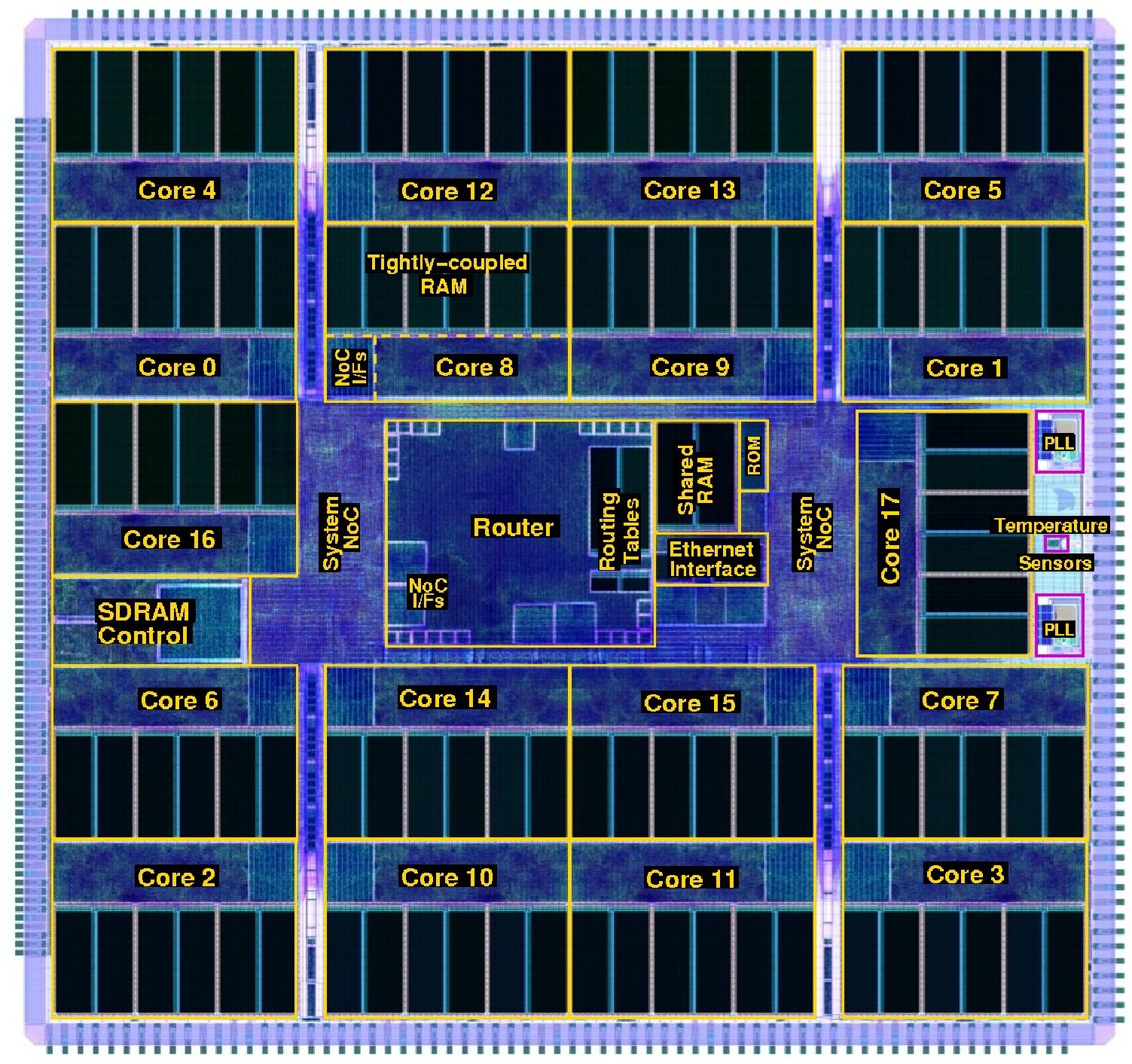 The SpiNNaker chip. Image credit: University of Manchester SpiNNaker boards and machines SpiNNaker chips (nodes) are interconnected using a two-dimensional toroidal triangular mesh, to create systems. Over the years, the SpiNNaker research team has designed and built increasingly larger boards and machines. The one million ARM cores machine is based on 1,200 boards, each containing forty-eight SpiNNaker chips. The boards occupy ten 19″ rack cabinets. 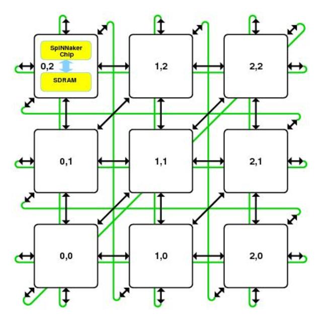 The SpiNNaker system architecture. Image credit: University of Manchester The community and the applications One hundred SpiNNaker machines are being used by research institutions around the world. An alternative way to access a large SpiNNaker machine is via the Human Brain Project portal. The HBP system will schedule jobs, allocating as much machine resource as is required by each job. To access SpiNNaker this way, users will need to join the HBP Community. Among the many applications, SpiNNaker machines have been used to obtain the first simulation of a cortical microcolumn (1mm2 cortex) and for many other researches in computational neuroscience, theoretical neuroscience and neurorobotics – as summarized by professor Furber’s presentation at NICE (Neuro Inspired Computational Elements) Workshop 2019. SpiNNaker2 Professor Furber also outlined the second phase of the project. The new chip will achieve a higher energy efficiency through 22FDX process technology and adaptive body biasing. Event driven operation with fine‐grained dynamic power management and energy proportional chip‐2‐chip links will allow for workload adaptivity. As described in a recent paper, each SpiNNaker2 chip will have 144 ARM M4F cores, augmented with hardware accelerators for random number generation and exponential functions. These resources, along with the floating point units available in the ARM cores, will enable SpiNNaker2 to mimic the brain’s process of synaptic rewiring and to use the reward-based synaptic sampling model, that employs structural plasticity to learn a function or task. According to the researchers, synaptic sampling cannot be directly implemented on other neuromorphic hardware with only static synapses or limited weight resolutions. SpiNNaker2 prototype test devices are available now, while tape-out of the final chip is scheduled for April 2020. Mark your calendar – and keep an eye on EDACafe for updates. |
|
|
|
||||||||
|
|||||||||
|
|||||||||


 Animation, 3D Art and 3D Models")