Processing hardware took center stage in August, with a number of announcements regarding AI chips, FPGAs, server processors, open source ISAs. As for the electronics industry in general, acquisition deals – one of them still in the making – attracted attention too.
The 1.2 trillion transistors chip
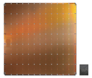
With more than 1.2 trillion transistors and an area of 46,225 square millimeters (8.5 x 8.5 inches), the Wafer Scale Engine (WSE) designed by Cerebras (Los Altos, CA) and manufactured by TSMC in its 16nm process technology is definitely an outstanding engineering achievement. Introduced at the Hot Chips conference – which took place at Stanford University from August 18 to 20 – the WSE is an Artificial Intelligence processor, aiming to compete against the GPUs commonly used for this type of applications. As Cerebras explained in a press release, it offers “400,000 AI-optimized, no-cache, no-overhead, compute cores and 18 gigabytes of local, distributed, superfast SRAM memory as the one and only level of the memory hierarchy. Memory bandwidth is 9 petabytes per second. The cores are linked together with a fine-grained, all-hardware, on-chip mesh-connected communication network that delivers an aggregate bandwidth of 100 petabits per second.” According to Cerebras, chip size is profoundly important to reduce training time and power in AI. A large silicon area provides more cores to do calculations, more memory closer to the cores, and the possibility to keep all communication on-silicon. One of the features specifically optimized for AI applications is the ‘sparsity harvesting technology’ invented by Cerebras, to boost performance on workloads that contain zeros. As the company explained, “Zeros are prevalent in deep learning calculations: often, the majority of the elements in the vectors and matrices that are to be multiplied together are zero. And yet multiplying by zero is a waste of silicon, power, and time (…). Because graphics processing units and tensor processing units are dense execution engines—engines designed to never encounter a zero—they multiply every element even when it is zero. When 50 to 98 percent of the data are zeros, as is often the case in deep learning, most of the multiplications are wasted.” Besides its significance from the AI point of view, the mega-chip is obviously interesting from a nanoelectronics technology standpoint: “The Cerebras WSE contains fundamental innovations that advance the state-of-the-art by solving decades-old technical challenges that limited chip size—such as cross-reticle connectivity, yield, power delivery, and packaging,” said Andrew Feldman, founder and CEO of Cerebras Systems.


