EDACafe Editorial Roberto Frazzoli
Roberto Frazzoli is a contributing editor to EDACafe. His interests as a technology journalist focus on the semiconductor ecosystem in all its aspects. Roberto started covering electronics in 1987. His weekly contribution to EDACafe started in early 2019. Cheating neural networks; Intel advanced packaging technologies; edge AI; faster verificationJuly 12th, 2019 by Roberto Frazzoli
What times we live in. Even neural networks cheat. Some have learnt to recognize a horse by spotting the tag www.pferdefotoarchiv.de, an archive of horse pictures; so if you paste this tag onto a Ferrari picture, the network will classify it as a horse. Some, when playing Atari Pinball game, have learnt to make high scores by repeatedly nudging the table, taking advantage of the high threshold of the tilting mechanism. Some have learnt to recognize airplanes just from the smooth blue landscape surrounding them in most pictures. These examples are among the results of a work carried out by a group of researchers from Fraunhofer Heinrich Hertz Institute and Technische Universität Berlin (Germany). Researchers used the layer-wise relevance propagation (LRP) method with the help of a semiautomatic tool called SpRAy (spectral relevance analysis), thus producing “heatmaps” where colors represent how important a certain pixels was for the neural network to make its decision (ranging from green, low relevance, to red, high relevance). As researchers observe, “The above cases exemplify our point, that even though test set error may be very low (or game scores very high), the reason for it may be due to what humans would consider as cheating rather than valid problem-solving behavior. It may not correspond to true performance when the latter is measured in a real-world environment, or when other criteria (e.g. social norms which penalize such behavior) are incorporated into the evaluation metric.”
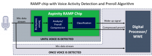
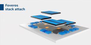
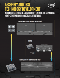
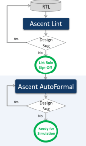
One of the most intriguing aspects of neural networks is their “black box” nature, in other words the fact that in many cases we don’t have a clear understanding of what’s going on inside them – even though we appreciate their performance. Most would agree that neural network research is still in its infancy; future developments will likely provide us with more insights – and new conceptual tools – to understand what happens in large neural networks. In the meantime, we need at least a way to explain their decision strategies. As observed by the researchers from Fraunhofer Heinrich Hertz Institute and Technische Universität Berlin, “Explanation techniques enable inspection of the decision process on a single instance basis. However, screening through a large number of individual explanations can be time consuming.” Hence, the use of a semiautomated technique – spectral relevance analysis – to efficiently investigate classifier behavior on large datasets. “SpRAy applies spectral clustering on a dataset of LRP explanations in order to identify typical, as well as atypical decision behaviors of the machine-learning model, and presents them to the user in a concise and interpretable manner.” Edge AI news AI applications are increasingly moving to edge devices, making this market very lively. BrainChip has recently signed a definitive agreement with Socionext America (SNA) for product development and manufacturing of its Akida Neuromorphic System-on-Chip. Headquartered in Santa Clara, California, Socionext America is a division of Japan-bsed Socionext Inc., the combination of the former Fujitsu and Panasonic System-on-Chip businesses. Socionext will provide turn-key ASIC services to BrainChip for the Akida product, including IP blocks for the external interfaces, the CPU Complex for internal control and data pre-processing, place and route of the integrated circuit, IP verification, final logic design, as well as managing wafer fabrication, assembly and test operations. Wafers will be provided by TSMC on its 28nm CMOS logic process. Another company in the edge AI space, Aspinity, is pursuing the “analyse-first” approach, targeting always-on sensing devices. Using a Reconfigurable Analog Modular Processor (RAMP), its solution analyzes raw analog sensor data for what’s important to the application, eliminating the higher-power processing and transmission of irrelevant data. According to the company, compared to a “digitize-first” architecture – where all sensor data must be continuously digitized for event analysis – the Aspinity approach reduces the power required by up to 10x and the volume of data handled by up to 100x. Intel advanced packaging news from Semicon West Chip packaging technologies are becoming increasingly important to integrate different dies (e.g. chiplets) in a single device. At Semicon West, that took place in San Francisco from July 9 to 11, Intel announced three updates to its advanced packaging capabilities, building upon its pre-existing EMIB (Embedded Multi-die Interconnect Bridge) and Foveros technologies. The company’s new Co-EMIB technology allows for the interconnection of two or more Foveros elements with essentially the performance of a single chip. A second technology called ODI (Omni-Directional Interconnect) is targeted at communication among chiplets in a package. The top chip can communicate horizontally with other chiplets, similar to EMIB. It can also communicate vertically with through-silicon vias (TSVs) in the base die below, similar to Foveros. ODI leverages large vertical vias to allow power delivery to the top die directly from the package substrate. Much larger than traditional TSVs, the large vias have lower resistance; this approach also reduces the number of TSVs required in the base die. The third technology, a new die-to-die interface called MDIO, builds upon Intel’s Advanced Interface Bus (AIB) PHY level interconnect. The solution enables a modular approach to system design with a library of chiplet intellectual property blocks. MDIO provides better power efficiency and more than double the pin speed and bandwidth density offered by AIB. Another innovation related to advanced packaging comes from the Austrian company EV Group, that has recently unveiled its Maskless Exposure (MLE) lithography technology. Also applicable to MEMS, biomedical and high-density printed circuit board applications, MLE targets high-volume manufacturing and claims to combine high-resolution patterning (<2 microns lines/spaces) with high throughput and yield, while eliminating the overhead costs associated with photomasks. Faster RTL verification from Real Intent Real Intent has announced that Ascent AutoFormal automatic RTL verification tool has been improved to provide 10X+ performance gains and analyze 5X larger designs when compared to the previous version. Other improvements include reduced turnaround time: detailed RTL design information that can impact the formal analysis is automatically provided before the tool start running. This ensures that relevant design elements are accurately analyzed in the first formal run, reducing iterations. For example, in addition to clocks and resets, the tool recognizes FSMs, and also identifies elements such as latches that could prevent the detection of the FSMs. |
|
|
|||||
|
|
|||||
|
|||||


