EDACafe Editorial Roberto Frazzoli
Roberto Frazzoli is a contributing editor to EDACafe. His interests as a technology journalist focus on the semiconductor ecosystem in all its aspects. Roberto started covering electronics in 1987. His weekly contribution to EDACafe started in early 2019. Major themes at SEMI ISS Europe: EUV lithography ready for volume production, challenges faced by the European industry, semiconductor market outlookApril 5th, 2019 by Roberto Frazzoli
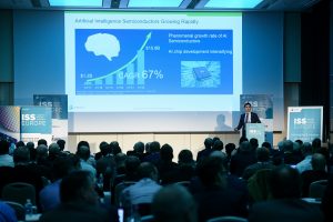
After a 33-year incubation, EUV lithography is finally ready for volume production: Samsung and TSMC will start using this technology to process more than 1,000 wafers per day – at 7 nanometers – during 2019. The announcement came from ASML – the Dutch company that developed the EUV lithography equipment – on occasion of the European “Industry Strategy Symposium” organized by SEMI, the global industry association representing the electronics manufacturing supply chain. This year the event took place in Milan, Italy, March 31st to April 2nd, and offered a picture of the challenges and opportunities facing the semiconductor industry in Europe. Back to single patterning Peter Jenkins from ASML summarized the long run that lead to EUV lithography, starting from the early researches in 1986 when this wavelength band was called “soft X-rays” – it was then re-branded “extreme ultraviolet” in 1993. A major boost came from the co-development agreement signed in 2012, when Intel, Samsung and TSMC joined ASML to provide additional resources. But a key piece of the puzzle was still missing to reach full scale productivity: a powerful EUV source. This roadblock was removed in 2013, when ASML acquired its EUV source supplier – Cymer – to help R&D on this front. Now, with 250-watt sources available, everything is in place. Jenkins stressed that EUV lithography allows to use single patterning even for the most advanced process nodes, thus reducing the manufacturing cost that has soared over the past few years due to double- and quadruple-patterning. New development and collaboration models required Given the key role played by ASML – headquartered in the Netherlands – EUV lithography is certainly a brilliant example of the European technological capabilities. But on many other hi-tech areas, Europe does not have a leading position and is facing significant challenges. Michael Alexander, from the strategy consulting firm Roland Berger, observed that there is a gap between the semiconductor industry and its OEM customers: chip makers are quite advanced in applying the latest “Industry 4.0” solutions in their fabs, while some European OEMs are not. To close this gap, the semiconductor industry should collaborate more closely with its OEM customers. New ways of working are needed even when the customer is as technologically advanced as the European automotive industry. Driving the change, in this case, is the disrupting effect of the increasing electronic content in cars. Burkhard Huhnke from Synopsys pointed out that recalls for electronics affects about five percent of the vehicles on the road, way too many if we want autonomous driving cars to become a reality. Part of the solution will be better testing through a “shift left” approach in the development of car electronics, that should take place in parallel to the development of the vehicle itself. Synopsys is enabling this by providing virtual ECUs (Electronic Control Units) that allow hardware-software co-design based on a model of the SoC, up to eighteen months before silicon is available. Another part of the solution will be adopting new SoC architectures to accommodate for the special requirements of car electronics, such as redundancy and compliance to ASIL-D safety standard. A recipe for European semiconductor startups One of the challenges that the European semiconductor industry is facing is an environment that is not favorable to startup companies. Loïc Lietar from Greenwaves – a startup specializing in low power IoT application processors, based in Grenoble, France – pointed out that semiconductor startups condense many of the features that venture capital does not like: long time to market, high risk, the need for experienced personnel. An additional problem in Europe is the lack of VC-firms specializing in semiconductors. But, above all, semiconductor startups have the bad reputation of being unreasonably capital intensive. The recipe that made Greenwaves successful is high capital efficiency – in other words, doing more with less money. This has been achieved in many ways: choosing a market with relatively short cycle times; starting with a mature process; gaining the trust of suppliers (e.g. IP vendors) to postpone payments; leveraging open source projects through academic collaborations (with ETH Zurich, Switzerland, and the University of Bologna, Italy). European Union initiatives supporting microelectronics Helping the European semiconductor industry to address all challenges, the European Union continues to provide R&D funds through a range of programs such as Ecsel, Penta and Silicon Europe. But other EU initiatives are pursuing the same goal: Mark Nicklas from the European Commission cited the support given to microelectronics within the IPCEI (Important Projects of Common European Interest) framework; Harald Gruber from the European Investment Bank stressed that this institution can play the role of venture capitalist to help startups overcome the ‘death valleys’ in their path to maturity. Gruber also observed that – compared to US – European young companies rely more on bank loans and less on equity, which makes innovation more difficult as a loan does not allow any risk-sharing. Headwinds in 2019, growth expectations for 2020 An injection of optimism comes from the current world market outlook. Clark Tseng from SEMI reminded that 2018 was a record year for semiconductors, with several chip makers investing in European fabs. Among them Intel, Infineon, STMicroelectronics, and Bosch – which is building a 300mm wafer fab in Dresden, Germany, that represents its single biggest investments since its foundation in 1886. Tsang expects headwinds in the first half of 2019 – due to challenges from macroeconomy, memory market slowdown and high inventory level – resulting in a minus 1% rate, but investment in leading-edge foundry and logic will continue, driven by growing demand for high-performance chips for AI and 5G. Therefore 2020 has the potential to be a new record year, with a forecasted +5.4% growth. With the participation of many significant companies of different sizes, the 2019 European SEMI’s Industry Strategy Symposium offered a rich program including many other speeches that cannot be summarized in this article. Among other things, SEMI’s president Ajit Manocha announced at the event new initiatives aimed at solving the talent shortage crisis. Category: EDACafe Editorial |
|
|
|||||
|
|
|||||
|
|||||


