Bit-Slice Design: Controllers and ALUs
by Donnamaie E. White
Copyright © 1996, 2001, 2002 Donnamaie E. White
- Pre-Introduction
- Selection of the Implementation
- Microprogramming
- Advantages of LSI
- The 2900 Family
- Language Interrelationships
- Controller Design
- Constructing the CCU
- Sequential Execution
- Multiple Sequences
- Start Addresses
- Mapping PROM
- Unconditional Branch
- Conditional Branch
- Timing Considerations
- Pipelining
- Improved Architecture
3. Adding Programming
Support to the Controller
- Expanded Testing
- Subroutines
- Nested Subroutines
- Stack Size
- Loops
- Am29811
- Am2909/11
- CASE Statement (Am29803A)
- Microprogram Memory
- Status Polling
- Interrupt Servicing
- Implementation - Interrupt Request Signals
- Vector Mapping PROM
- Next Address Control
- Am2910
- Am2910 Instructions
- Control Lines
- Interrupt Handling
- Am2914
- Interconnection of the Am2914
6. The ALU and Basic Arithmetic
- Further Enhancements
- Instruction Fields
- Instruction Set Extensions
- Sample Operations
- Arithmetic -- General
- Multiplication with the Am2901
- Am2903 Multiply
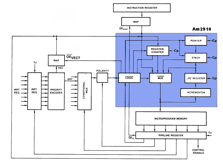
Refining the CCULast Edit November 2, 1996; May 1, 1999; July 7, 2001 AMD's Am2910 - A Slick Control SolutionFigure 4-7 AMD's Am2910 Supersequencer - now obsolete - solved many of the CCU construction problems
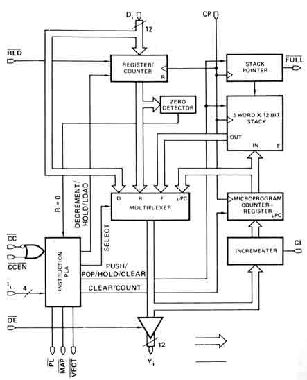
Am2910The block diagram of the Am2910 is shown in Figure 4-8. This device is controlled by a 4-bit instruction, which would be supplied from one field of the microword format of the system. These four bits provide 16 basic instructions, which are similar but not identical with Am29811A instructions. They are discussed in detail in this chapter. Figure 4-8 Am2910 Block Diagram
The Am2910 can address up to 4K of PROM/ROM memory. Unused address lines are left floating at the output; the corresponding Di inputs should be tied to ground. It provides three output enables controls: PL', MAP', and VECT' (all are complementary - i.e., should have overbars). The 4-bit instruction, the result of the CC', CCEN' inputs and the internal zero detect for the register/counter all are inputs to an onboard instruction PLA (programmable logic array). The PLA provides the internal controls which correspond to the next-address control logic. The next address can be from one of four sources:
Di is connected to the tristated outputs of the vector map, the mapping PROM, and the pipeline in the example CCU developed so far.
|