|
|||||||||||||||||||||||||||||||||||||||||||||||||||||||||||||||||||||||||||||||||||||||||||||||||||||||||||||||||||||||
|
[ Chapter start ] [ Previous page ] [ Next page ] 2.4 Combinational Logic CellsThe AND-OR-INVERT (AOI) and the OR-AND-INVERT (OAI) logic cells are particularly efficient in CMOS. Figure 2.12 shows an AOI221 and an OAI321 logic cell (the logic symbols in Figure 2.12 are not standards, but are widely used). All indices (the indices are the numbers after AOI or OAI) in the logic cell name greater than 1 correspond to the inputs to the first “level” or stage—the AND gate(s) in an AOI cell, for example. An index of '1' corresponds to a direct input to the second-stage cell. We write indices in descending order; so it is AOI221 and not AOI122 (but both are equivalent cells), and AOI32 not AOI23. If we have more than one direct input to the second stage we repeat the '1'; thus an AOI211 cell performs the function Z = (A.B + C + D)'. A three-input NAND cell is an OAI111, but calling it that would be very confusing. These rules are not standard, but form a convention that we shall adopt and one that is widely used in the ASIC industry. There are many ways to represent the logical operator, AND. I shall use the middle dot and write A · B (rather than AB, A.B, or A ∧ B); occasionally I may use AND(A, B). Similarly I shall write A + B as well as OR(A, B). I shall use an apostrophe like this, A', to denote the complement of A rather than A since sometimes it is difficult or inappropriate to use an overbar ( vinculum ) or diacritical mark (macron). It is possible to misinterpret AB' as A B rather than AB (but the former alternative would be A · B' in my convention). I shall be careful in these situations.
We can express the function of the AOI221 cell in Figure 2.12(a) as We can also write this equation unambiguously as Z = OAI221(A, B, C, D, E), just as we might write X = NAND (I, J, K) to describe the logic function X = (I · J · K)'. This notation is useful because, for example, if we write OAI321(P, Q, R, S, T, U) we immediately know that U (the sixth input) is the (only) direct input connected to the second stage. Sometimes we need to refer to particular inputs without listing them all. We can adopt another convention that letters of the input names change with the index position. Now we can refer to input B2 of an AOI321 cell, for example, and know which input we are talking about without writing Table 2.10 shows the AOI family of logic cells with three indices (with branches in the family for AOI, OAI, AO, and OA cells). There are 5 types and 14 separate members of each branch of this family. There are thus 4 ¥ 14 = 56 cells of the type X abc where X = {OAI, AOI, OA, AO} and each of the indexes a , b , and c can range from 1 to 3. We form the AND-OR (AO) and OR-AND (OA) cells by adding an inverter to the output of an AOI or OAI cell.
2.4.1 Pushing BubblesThe AOI and OAI logic cells can be built using a single stage in CMOS using series–parallel networks of transistors called stacks. Figure 2.13 illustrates the procedure to build the n -channel and p -channel stacks, using the AOI221 cell as an example. Here are the steps to construct any single-stage combinational CMOS logic cell:
The two stacks are network duals (they can be derived from each other by swapping series connections for parallel, and parallel for series connections). The n -channel stack implements the strong '0's of the function and the p -channel stack provides the strong '1's. The final step is to adjust the drive strength of the logic cell by sizing the transistors. 2.4.2 Drive StrengthNormally we ratio the sizes of the n -channel and p -channel transistors in an inverter so that both types of transistors have the same resistance, or drive strength . That is, we make b n = b p . At low dopant concentrations and low electric fields m n is about twice m p . To compensate we make the shape factor, W/L, of the p -channel transistor in an inverter about twice that of the n -channel transistor (we say the logic has a ratio of 2). Since the transistor lengths are normally equal to the minimum poly width for both types of transistors, the ratio of the transistor widths is also equal to 2. With the high dopant concentrations and high electric fields in submicron transistors the difference in mobilities is less—typically between 1 and 1.5. Logic cells in a library have a range of drive strengths. We normally call the minimum-size inverter a 1X inverter. The drive strength of a logic cell is often used as a suffix; thus a 1X inverter has a cell name such as INVX1 or INVD1. An inverter with transistors that are twice the size will be an INVX2. Drive strengths are normally scaled in a geometric ratio, so we have 1X, 2X, 4X, and (sometimes) 8X or even higher, drive-strength cells. We can size a logic cell using these basic rules:
For example, a transistor with shape factor 3/1 (we shall call this “a 3/1”) in series with another 3/1 is equivalent to a 1/((1/3) + (1/3)) or a 3/2. We can use the following method to calculate equivalent transistor sizes:
We have to be careful to keep W and L reasonable. For example, a 3/1 in series with a 2/1 is equivalent to a 1/((1/3) + (1/2)) or 1/0.83. Since we cannot make a device 2 l wide and 1.66 l long, a 1/0.83 is more naturally written as 3/2.5. We like to keep both W and L as integer multiples of 0.5 (equivalent to making W and L integer multiples of l ), but W and L must be greater than 1. In Figure 2.13(c) the transistors in the AOI221 cell are sized so that any string through the p -channel stack has a drive strength equivalent to a 2/1 p -channel transistor (we choose the worst case, if more than one transistor in parallel is conducting then the drive strength will be higher). The n -channel stack is sized so that it has a drive strength of a 1/1 n -channel transistor. The ratio in this library is thus 2. If we were to use four drive strengths for each of the AOI family of cells shown in Table 2.10, we would have a total of 224 combinational library cells—just for the AOI family. The synthesis tools can handle this number of cells, but we may not be able to design this many cells in a reasonable amount of time. Section 3.3, “Logical Effort,” will help us choose the most logically efficient cells. 2.4.3 Transmission GatesFigure 2.14(a) and (b) shows a CMOS transmission gate ( TG , TX gate, pass gate, coupler). We connect a p -channel transistor (to transmit a strong '1') in parallel with an n -channel transistor (to transmit a strong '0').
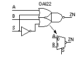
We can express the function of a TG as but this is ambiguous—if we write TG(X, Y), how do we know if X is connected to the gates or sources/drains of the TG? We shall always define TG(X, Y) when we use it. It is tempting to write TG(A, S) = A · S, but what is the value of Z when S ='0' in Figure 2.14(a), since Z is then left floating? A TG is a switch, not an AND logic cell. There is a potential problem if we use a TG as a switch connecting a node Z that has a large capacitance, C BIG , to an input node A that has only a small capacitance C SMALL (see Figure 2.14c). If the initial voltage at A is V SMALL and the initial voltage at Z is V BIG , when we close the TG (by setting S = '1') the final voltage on both nodes A and Z is Imagine we want to drive a '0' onto node Z from node A. Suppose C BIG = 0.2 pF (about 10 standard loads in a 0.5 m m process) and C SMALL = 0.02 pF, V BIG = 0 V and V SMALL = 5 V; then This is not what we want at all, the “big” capacitor has forced node A to a voltage close to a '0'. This type of problem is known as charge sharing . We should make sure that either (1) node A is strong enough to overcome the big capacitor, or (2) insulate node A from node Z by including a buffer (an inverter, for example) between node A and node Z. We must not use charge to drive another logic cell—only a logic cell can drive a logic cell. If we omit one of the transistors in a TG (usually the p -channel transistor) we have a pass transistor . There is a branch of full-custom VLSI design that uses pass-transistor logic. Much of this is based on relay-based logic, since a single transistor switch looks like a relay contact. There are many problems associated with pass-transistor logic related to charge sharing, reduced noise margins, and the difficulty of predicting delays. Though pass transistors may appear in an ASIC cell inside a library, they are not used by ASIC designers. We can use two TGs to form a multiplexer (or multiplexor—people use both orthographies) as shown in Figure 2.15(a). We often shorten multiplexer to MUX . The MUX function for two data inputs, A and B, with a select signal S, is We can write this as Z = A · S' + B · S, since node Z is always connected to one or other of the inputs (and we assume both are driven). This is a two-input MUX (2-to-1 MUX or 2:1 MUX). Unfortunately, we can also write the MUX function as Z = A · S + B · S', so it is difficult to write the MUX function unambiguously as Z = MUX(X, Y, Z). For example, is the select input X, Y, or Z? We shall define the function MUX(X, Y, Z) each time we use it. We must also be careful to label a MUX if we use the symbol shown in Figure 2.15(b). Symbols for a MUX are shown in Figure 2.15(b–d). In the IEEE notation 'G' specifies an AND dependency. Thus, in Figure 2.15(c), G = '1' selects the input labeled '1'. Figure 2.15(d) uses the common control block symbol (the notched rectangle). Here, G1 = '1' selects the input '1', and G1 = '0' selects the input ' 1 '. Strictly this form of IEEE symbol should be used only for elements with more than one section controlled by common signals, but the symbol of Figure 2.15(d) is used often for a 2:1 MUX. The MUX shown in Figure 2.15(a) works, but there is a potential charge-sharing problem if we cascade MUXes (connect them in series). Instead most ASIC libraries use MUX cells built with a more conservative approach. We could buffer the output using an inverter (Figure 2.15e), but then the MUX becomes inverting. To build a safe, noninverting MUX we can buffer the inputs and output (Figure 2.15f)—requiring 12 transistors, or 3 gate equivalents (only the gate equivalent counts are shown from now on). Figure 2.16 shows how to use an OAI22 logic cell (and an inverter) to implement an inverting MUX. The implementation in equation form (2.5 gates) is (both A' and NOT(A) represent an inverter, depending on which representation is most convenient—they are equivalent). I often use an equation to describe a cell implementation. The following factors will determine which MUX implementation is best:
A minimum-size TG is a little slower than a minimum-size inverter, so there is not much difference between the implementations shown in Figure 2.15 and Figure 2.16, but the difference can become important for 4:1 and larger MUXes. 2.4.4 Exclusive-OR CellThe two-input exclusive-OR ( XOR , EXOR, not-equivalence, ring-OR) function is We are now using multiletter symbols, but there should be no doubt that A1' means anything other than NOT(A1). We can implement a two-input XOR using a MUX and an inverter as follows (2 gates): This implementation only buffers one input and does not buffer the MUX output. We can use inverter buffers (3.5 gates total) or an inverting MUX so that the XOR cell does not have any external connections to source/drain diffusions as follows (3 gates total): We can also implement a two-input XOR using an AOI21 (and a NOR cell), since (2.5 gates). Similarly we can implement an exclusive-NOR (XNOR, equivalence) logic cell using an inverting MUX (and two inverters, total 3.5 gates) or an OAI21 logic cell (and a NAND cell, total 2.5 gates) as follows (using the MUX function of Eq. 2.34): [ Chapter start ] [ Previous page ] [ Next page ] | |||||||||||||||||||||||||||||||||||||||||||||||||||||||||||||||||||||||||||||||||||||||||||||||||||||||||||||||||||||||


 Animation, 3D Art and 3D Models")